Instructor: Lei He
Email: LHE@ee.ucla.edu
- Главная
- Разное
- Дизайн
- Бизнес и предпринимательство
- Аналитика
- Образование
- Развлечения
- Красота и здоровье
- Финансы
- Государство
- Путешествия
- Спорт
- Недвижимость
- Армия
- Графика
- Культурология
- Еда и кулинария
- Лингвистика
- Английский язык
- Астрономия
- Алгебра
- Биология
- География
- Детские презентации
- Информатика
- История
- Литература
- Маркетинг
- Математика
- Медицина
- Менеджмент
- Музыка
- МХК
- Немецкий язык
- ОБЖ
- Обществознание
- Окружающий мир
- Педагогика
- Русский язык
- Технология
- Физика
- Философия
- Химия
- Шаблоны, картинки для презентаций
- Экология
- Экономика
- Юриспруденция
Interconnect delay. (Chapter 7) презентация
Содержание
- 1. Interconnect delay. (Chapter 7)
- 2. Chapter 7 Interconnect Delay 7.1 Elmore Delay
- 3. Basic Circuit Analysis Techniques Output response
- 4. unit step function u(t)= 0 1
- 5. Definitions: (unit) step input u(t)
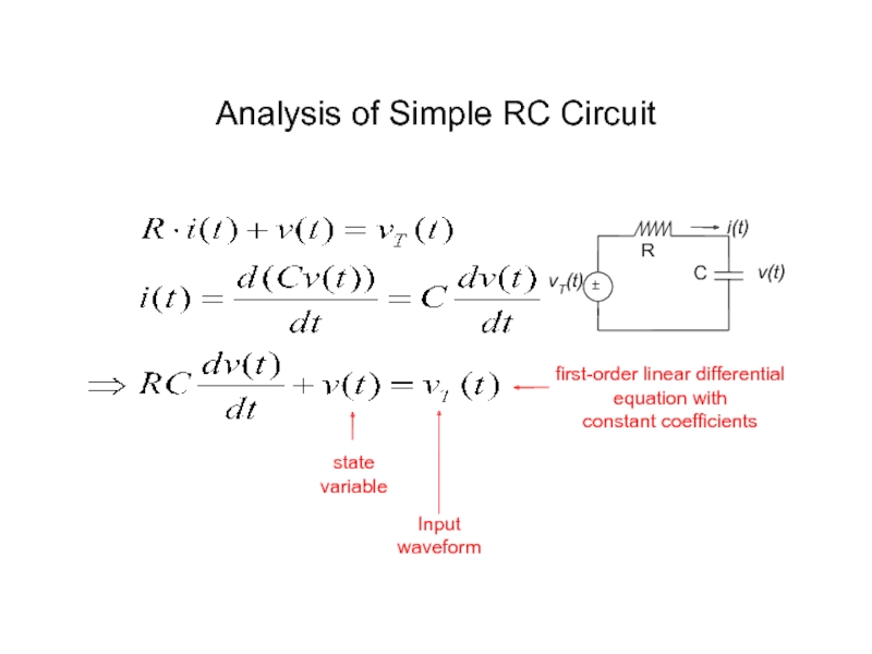
- 6. Analysis of Simple RC Circuit first-order linear
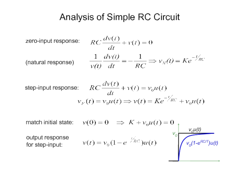
- 7. Analysis of Simple RC Circuit zero-input response:
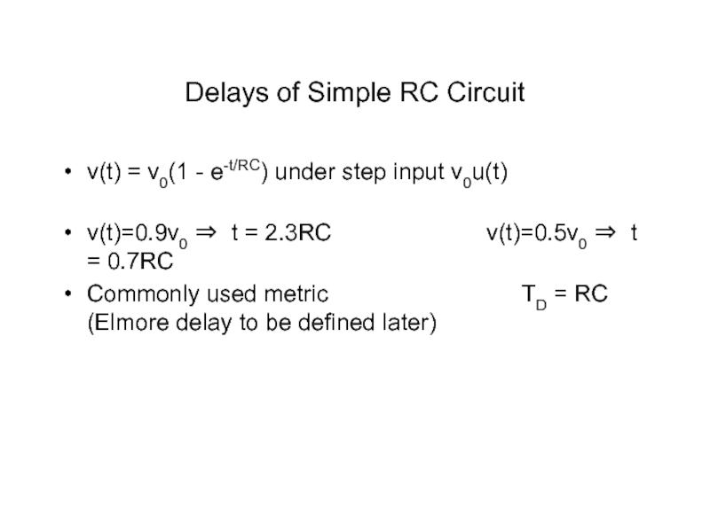
- 8. Delays of Simple RC Circuit v(t) =
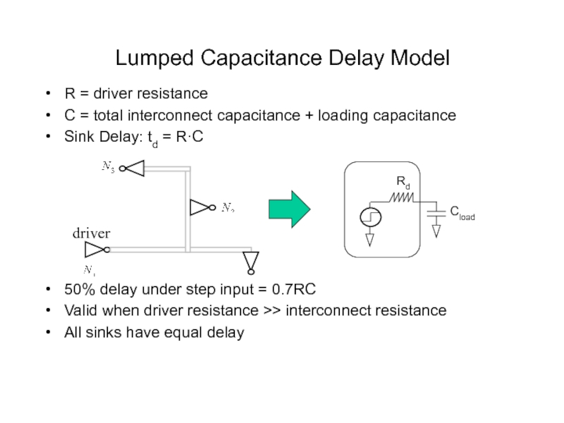
- 9. Lumped Capacitance Delay Model R = driver
- 11. Delay of Distributed RC Lines Vout(t) Vout(s)
- 12. Delay of Distributed RC Lines (cont’d)
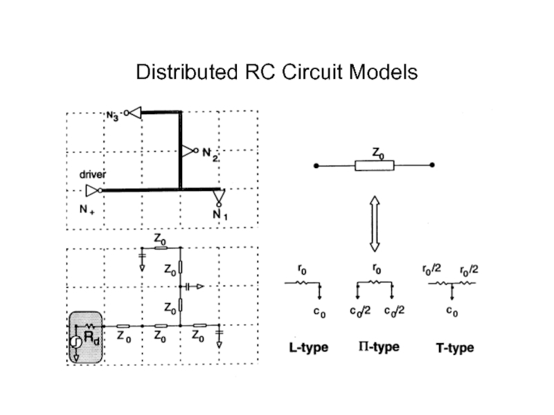
- 13. Distributed Interconnect Models Distributed RC circuit model
- 14. Distributed RC Circuit Models
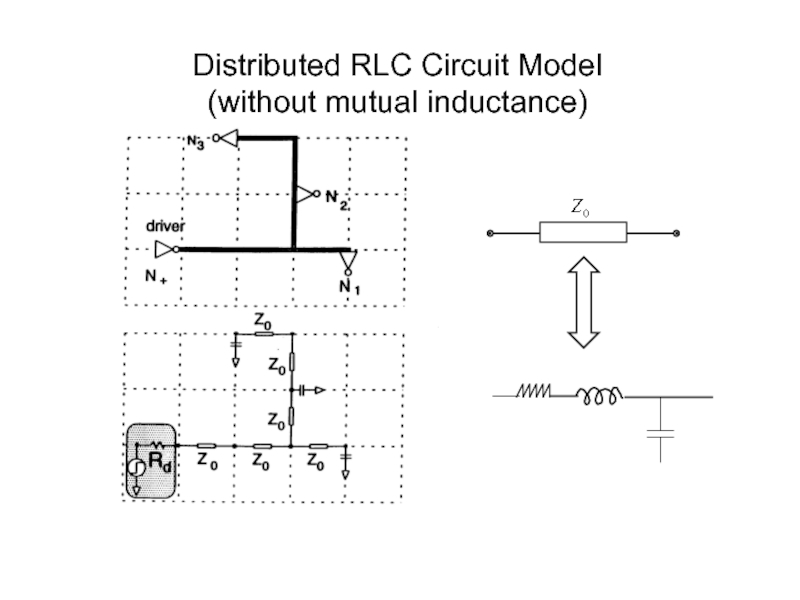
- 15. Distributed RLC Circuit Model (without mutual inductance)
- 16. Delays of Complex Circuits under Unit Step
- 17. Delays of Complex Circuits under Unit Step
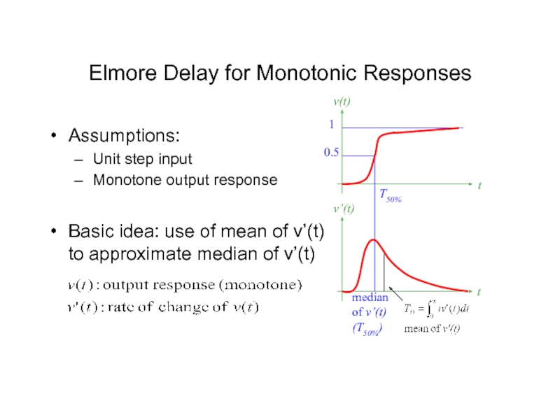
- 18. 0.5 1 T50% v(t) t t
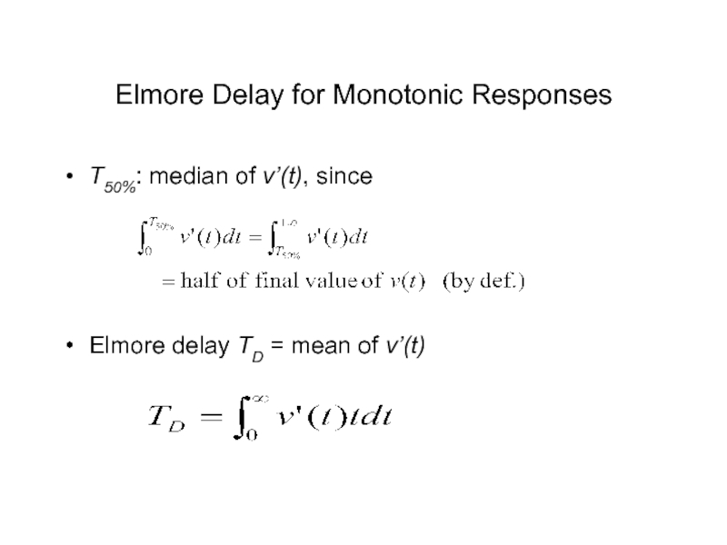
- 19. T50%: median of v’(t), since
- 20. Why Elmore Delay? Elmore delay is easier
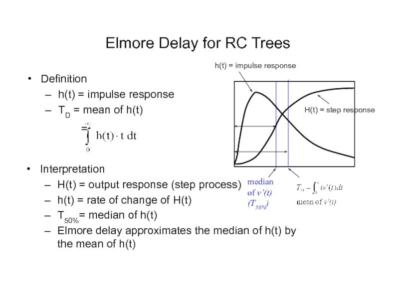
- 21. Elmore Delay for RC Trees Definition h(t)
- 22. Elmore Delay of a RC Tree [Rubinstein-Penfield-Horowitz,
- 23. Elmore Delay in a RC Tree (cont’d)
- 24. Elmore Delay in a RC Tree (cont’d)
- 25. Some Definitions For Signal Bound Computation
- 26. Signal Bounds in RC Trees Theorem
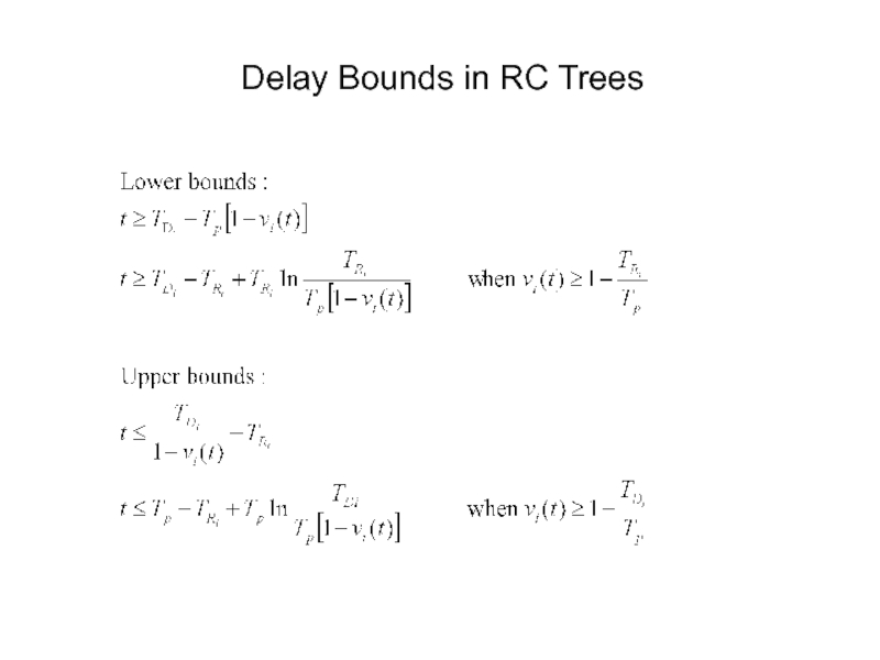
- 27. Delay Bounds in RC Trees
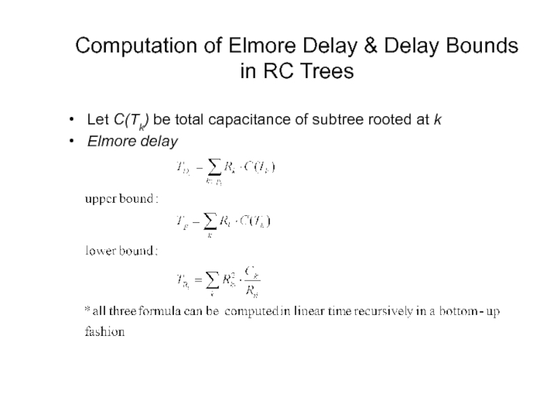
- 28. Computation of Elmore Delay & Delay Bounds
- 29. Comments on Elmore Delay Model Advantages Simple
- 30. Comments on Elmore Delay Model Disadvantages Low
- 31. Chapter 7.2 Higher-order Delay Model
- 32. Time Moments of Impulse Response h(t) Definition
- 33. Pade Approximation H(s) can be modeled
- 34. General Moment Matching Technique Basic idea: match
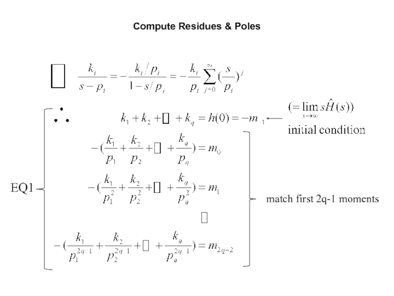
- 35. Compute Residues & Poles match first 2q-1 moments EQ1
- 36. Basic Steps for Moment Matching Step 1:
- 37. Components of Moment Matching Model Moment computation
- 38. Chapter 7 Interconnect Delay 7.1 Elmore Delay
- 39. Stage Delay A B C Source Interconnect Load
- 40. Modeling of Capacitive Load First-order approximation: the
- 41. Π-Model [O’Brian-Savarino, ICCAD’89] Moment matching again! Consider
- 42. Driving-Point Admittance Approximations Driving-point admittance = Sum
- 43. Driving-Point Admittance Approximations First order approximation: y(1)
- 44. Third Order Approximation: Π Model
- 45. Current Moment Computation Similar to the voltage
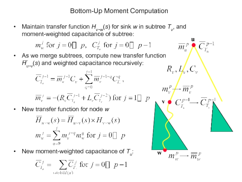
- 46. Bottom-Up Moment Computation Maintain transfer function Hv~w(s)
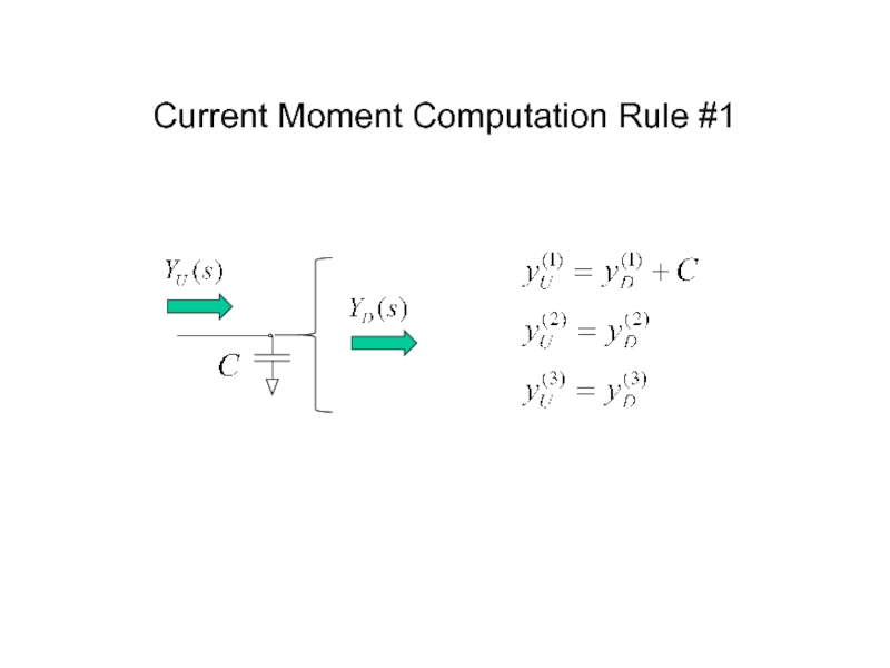
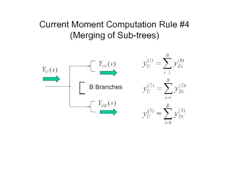
- 47. Current Moment Computation Rule #1
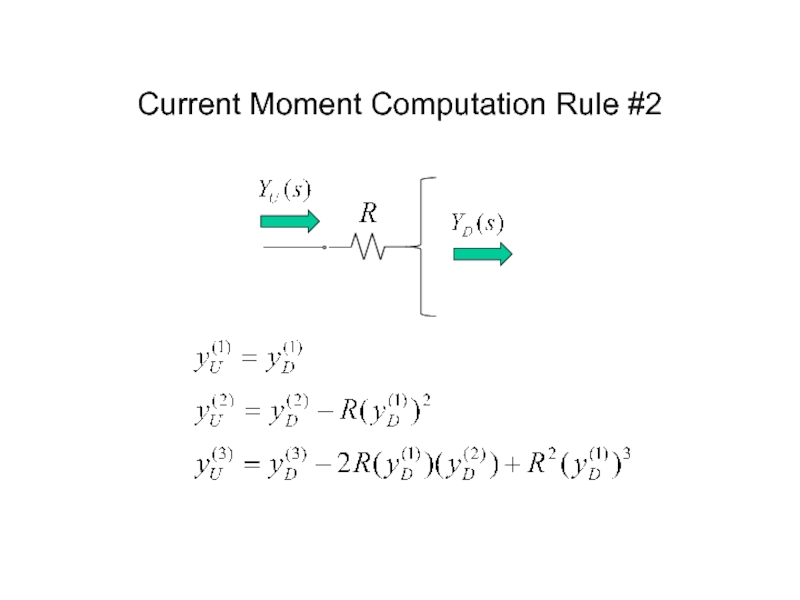
- 48. Current Moment Computation Rule #2
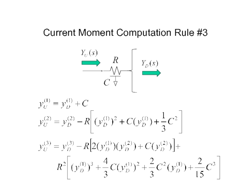
- 49. Current Moment Computation Rule #3
- 50. Current Moment Computation Rule #4 (Merging of Sub-trees) B Branches
- 51. Example:
- 52. Why Effective Capacitance Model? The π-model is
- 53. Equating Average Currents tD =
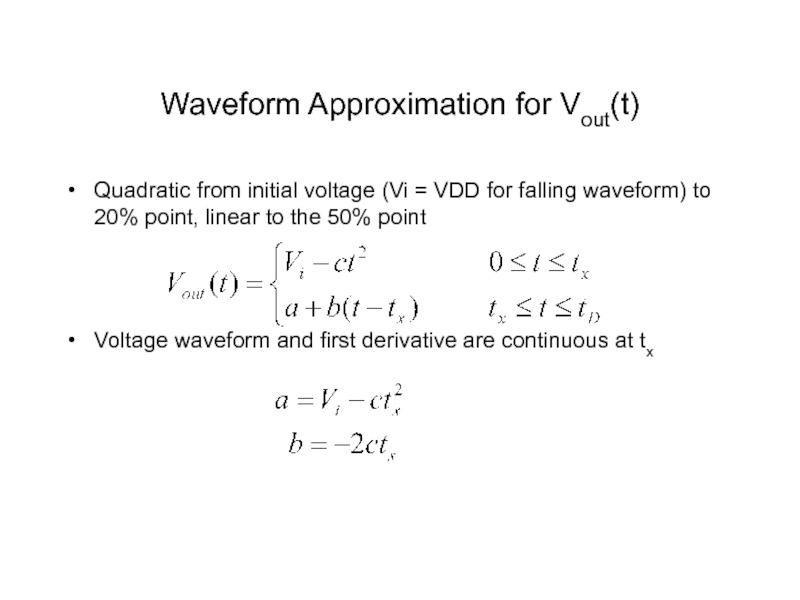
- 54. Waveform Approximation for Vout(t) Quadratic from initial
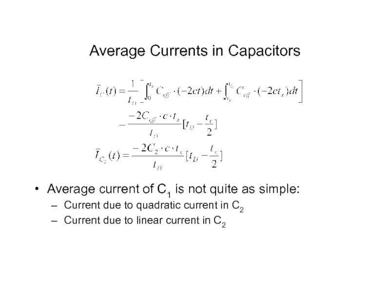
- 55. Average Currents in Capacitors Average current of
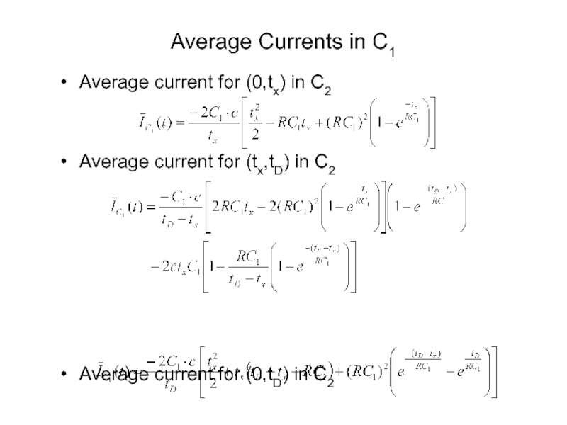
- 56. Average current for (0,tx) in C2
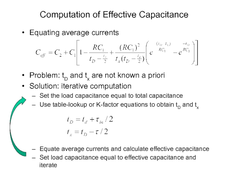
- 57. Computation of Effective Capacitance Equating average currents
- 58. Stage Delay Computation Calculate output waveform
Слайд 1EE 201A (Starting 2005, called EE 201B) Modeling and Optimization for VLSI Layout
Слайд 2Chapter 7 Interconnect Delay
7.1 Elmore Delay
7.2 High-order model and moment matching
7.3
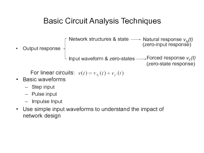
Слайд 3Basic Circuit Analysis Techniques
Output response
Basic waveforms
Step input
Pulse input
Impulse Input
Use simple input
Network structures & state
Input waveform & zero-states
Natural response vN(t)
(zero-input response)
Forced response vF(t)
(zero-state response)
For linear circuits:
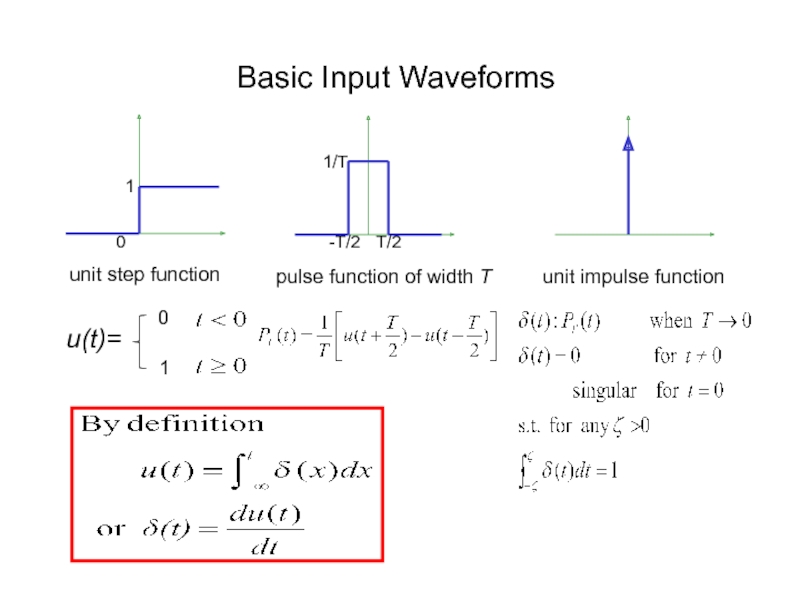
Слайд 4unit step function
u(t)=
0
1
1
pulse function of width T
0
1/T
-T/2
T/2
unit impulse function
Basic Input Waveforms
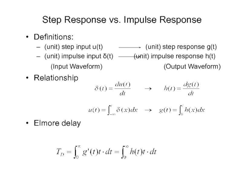
Слайд 5Definitions:
(unit) step input u(t)
(unit) impulse input δ(t) (unit) impulse response h(t)
Relationship
Elmore delay
Step Response vs. Impulse Response
(Input Waveform)
(Output Waveform)
Слайд 6Analysis of Simple RC Circuit
first-order linear differential
equation with
constant coefficients
state variable
Input
waveform
Слайд 7Analysis of Simple RC Circuit
zero-input response:
(natural response)
step-input response:
match initial state:
output response
for
Слайд 8Delays of Simple RC Circuit
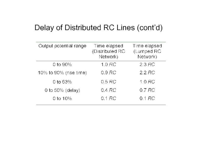
v(t) = v0(1 - e-t/RC) under step
v(t)=0.9v0 ⇒ t = 2.3RC v(t)=0.5v0 ⇒ t = 0.7RC
Commonly used metric TD = RC (Elmore delay to be defined later)
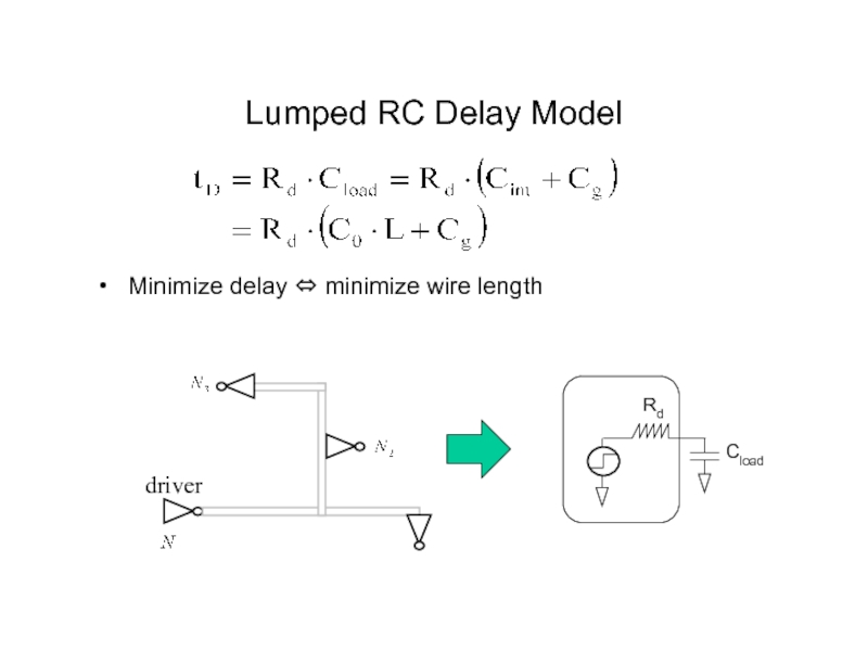
Слайд 9Lumped Capacitance Delay Model
R = driver resistance
C = total interconnect capacitance
Sink Delay: td = R·C
50% delay under step input = 0.7RC
Valid when driver resistance >> interconnect resistance
All sinks have equal delay
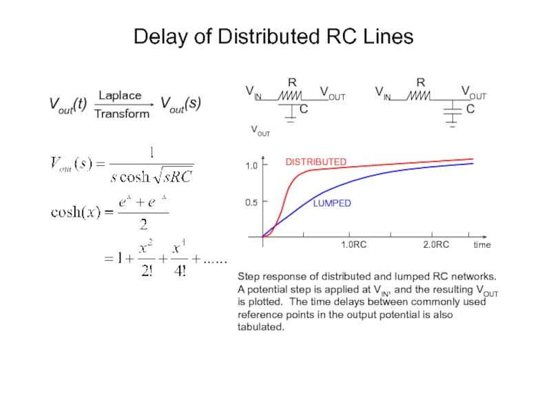
Слайд 11Delay of Distributed RC Lines
Vout(t)
Vout(s)
Laplace
Transform
R
VIN
VOUT
C
VOUT
VIN
R
C
0.5
1.0
VOUT
DISTRIBUTED
LUMPED
1.0RC
2.0RC
time
Step response of distributed and lumped RC
A potential step is applied at VIN, and the resulting VOUT
is plotted. The time delays between commonly used
reference points in the output potential is also tabulated.
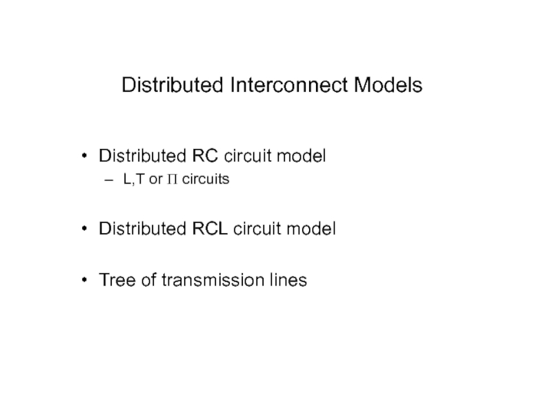
Слайд 13Distributed Interconnect Models
Distributed RC circuit model
L,T or Π circuits
Distributed RCL circuit
Tree of transmission lines
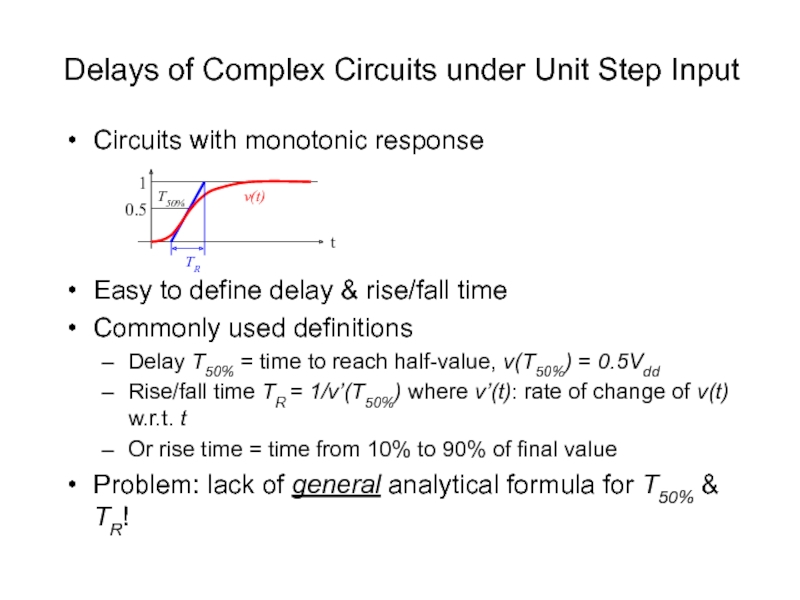
Слайд 16Delays of Complex Circuits under Unit Step Input
Circuits with monotonic response
Easy
Commonly used definitions
Delay T50% = time to reach half-value, v(T50%) = 0.5Vdd
Rise/fall time TR = 1/v’(T50%) where v’(t): rate of change of v(t) w.r.t. t
Or rise time = time from 10% to 90% of final value
Problem: lack of general analytical formula for T50% & TR!
t
1
0.5
v(t)
T50%
TR
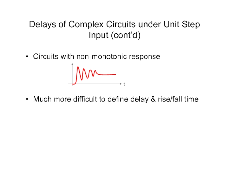
Слайд 17Delays of Complex Circuits under Unit Step Input (cont’d)
Circuits with non-monotonic
Much more difficult to define delay & rise/fall time
Слайд 18
0.5
1
T50%
v(t)
t
t
v’(t)
median
of v’(t)
(T50%)
Elmore Delay for Monotonic Responses
Assumptions:
Unit step input
Monotone output response
Basic
Слайд 19T50%: median of v’(t), since
Elmore delay TD = mean of v’(t)
Elmore
Слайд 20Why Elmore Delay?
Elmore delay is easier to compute analytically in most
Elmore’s insight [Elmore, J. App. Phy 1948]
Verified later on by many other researchers, e.g.
Elmore delay for RC trees [Penfield-Rubinstein, DAC’81]
Elmore delay for RC networks with ramp input [Chan, T-CAS’86]
.....
For RC trees: [Krauter-Tatuianu-Willis-Pileggi, DAC’95] T50% ≤ TD
Note: Elmore delay is not 50% value delay in general!
Слайд 21Elmore Delay for RC Trees
Definition
h(t) = impulse response
TD = mean of
=
Interpretation
H(t) = output response (step process)
h(t) = rate of change of H(t)
T50%= median of h(t)
Elmore delay approximates the median of h(t) by the mean of h(t)
median
of v’(t)
(T50%)
h(t) = impulse response
H(t) = step response
Слайд 22Elmore Delay of a RC Tree
[Rubinstein-Penfield-Horowitz, T-CAD’83]
Lemma:
Proof:
Apply impulse func. at t=0:
imin
i
current
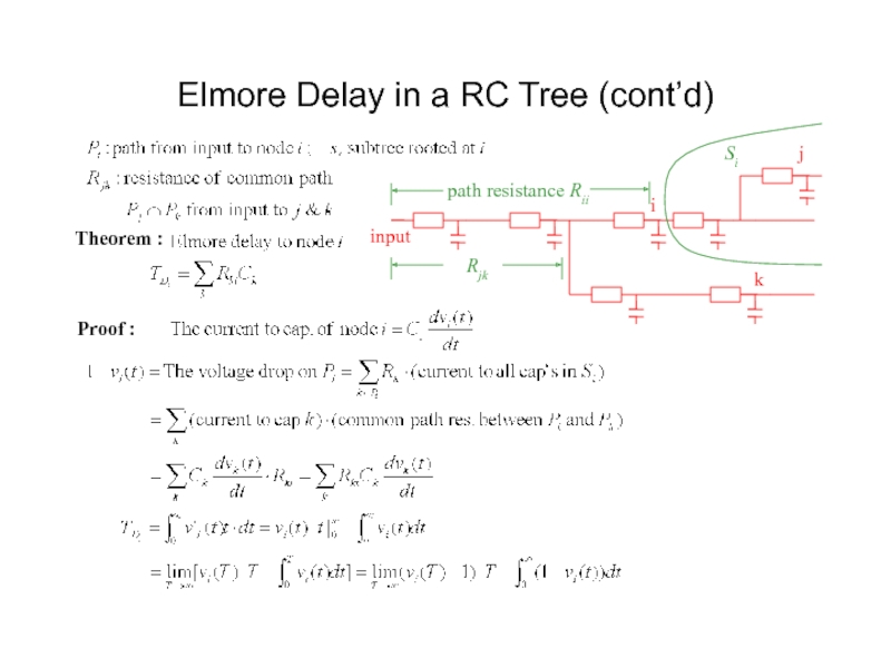
Слайд 24Elmore Delay in a RC Tree (cont’d)
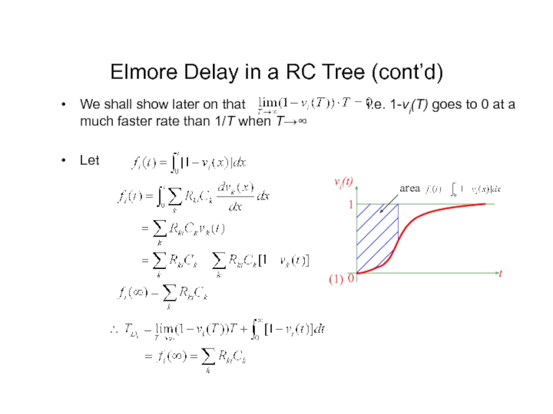
We shall show later on
Let
(1)
vi(t)
1
0
t
area
Слайд 28Computation of Elmore Delay & Delay Bounds in RC Trees
Let C(Tk)
Elmore delay
Слайд 29Comments on Elmore Delay Model
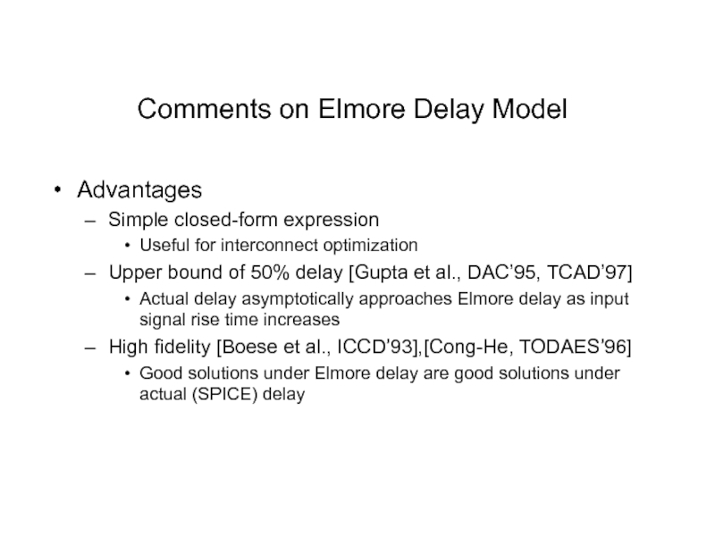
Advantages
Simple closed-form expression
Useful for interconnect optimization
Upper bound
Actual delay asymptotically approaches Elmore delay as input signal rise time increases
High fidelity [Boese et al., ICCD’93],[Cong-He, TODAES’96]
Good solutions under Elmore delay are good solutions under actual (SPICE) delay
Слайд 30Comments on Elmore Delay Model
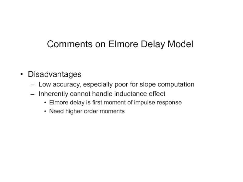
Disadvantages
Low accuracy, especially poor for slope computation
Inherently
Elmore delay is first moment of impulse response
Need higher order moments
Слайд 32Time Moments of Impulse Response h(t)
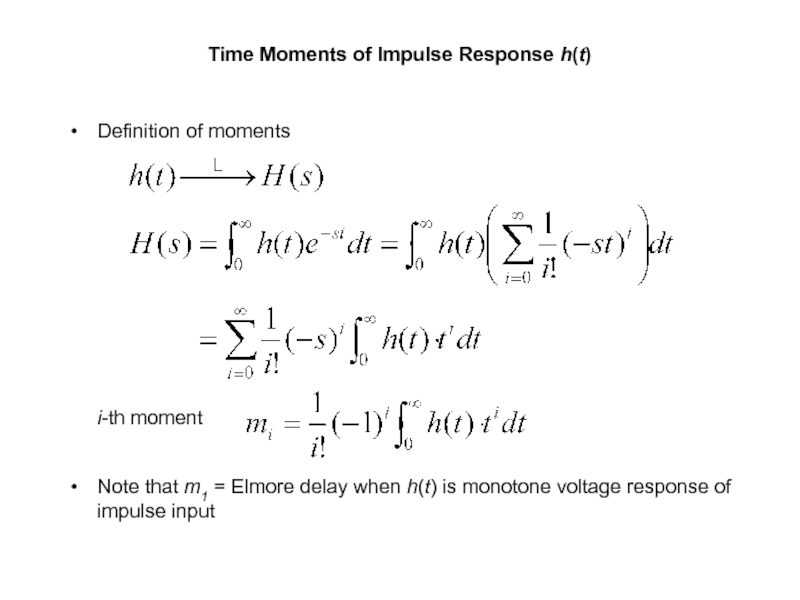
Definition of moments
i-th moment
Note that m1
Слайд 33Pade Approximation
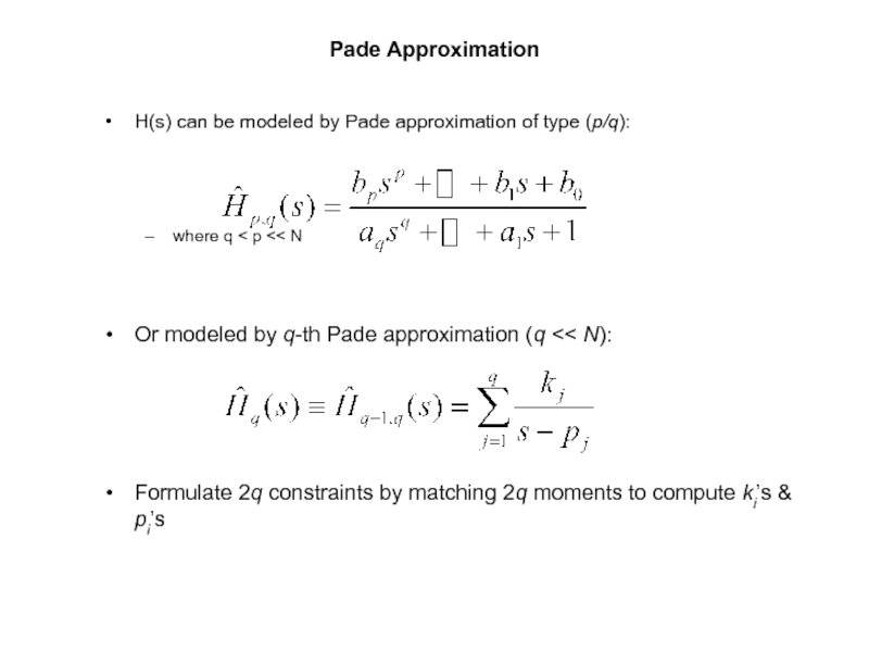
H(s) can be modeled by Pade approximation of type
where q < p << N
Or modeled by q-th Pade approximation (q << N):
Formulate 2q constraints by matching 2q moments to compute ki’s & pi’s
Слайд 34General Moment Matching Technique
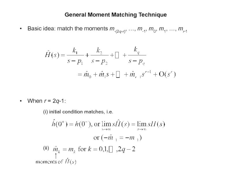
Basic idea: match the moments m-(2q-r), …, m-1,
(i) initial condition matches, i.e.
When r = 2q-1:
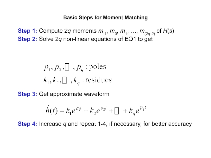
Слайд 36Basic Steps for Moment Matching
Step 1: Compute 2q moments m-1, m0,
Step 2: Solve 2q non-linear equations of EQ1 to get
Step 3: Get approximate waveform
Step 4: Increase q and repeat 1-4, if necessary, for better accuracy
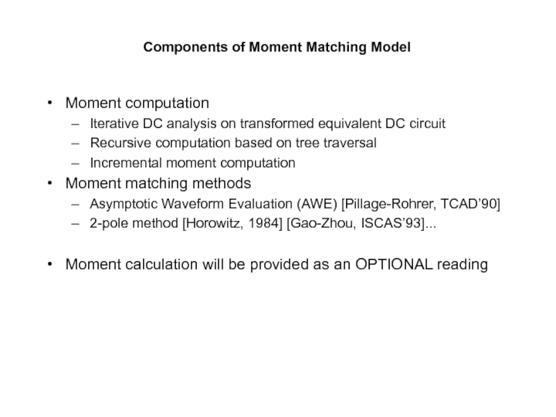
Слайд 37Components of Moment Matching Model
Moment computation
Iterative DC analysis on transformed equivalent
Recursive computation based on tree traversal
Incremental moment computation
Moment matching methods
Asymptotic Waveform Evaluation (AWE) [Pillage-Rohrer, TCAD’90]
2-pole method [Horowitz, 1984] [Gao-Zhou, ISCAS’93]...
Moment calculation will be provided as an OPTIONAL reading
Слайд 38Chapter 7 Interconnect Delay
7.1 Elmore Delay
7.2 High-order model and moment matching
7.3
Слайд 40Modeling of Capacitive Load
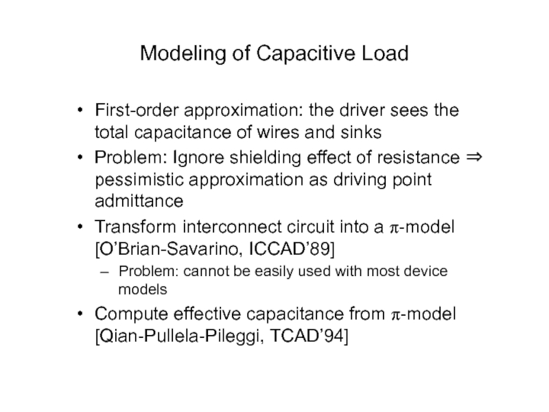
First-order approximation: the driver sees the total capacitance
Problem: Ignore shielding effect of resistance ⇒ pessimistic approximation as driving point admittance
Transform interconnect circuit into a π-model [O’Brian-Savarino, ICCAD’89]
Problem: cannot be easily used with most device models
Compute effective capacitance from π-model [Qian-Pullela-Pileggi, TCAD’94]
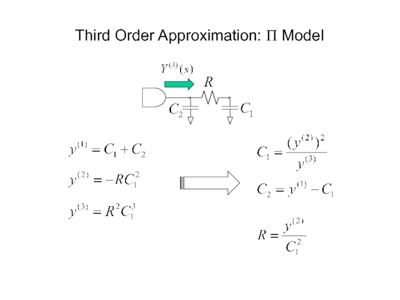
Слайд 41Π-Model
[O’Brian-Savarino, ICCAD’89]
Moment matching again!
Consider the first three moments of driving point
Current in the downstream of node k
Слайд 42Driving-Point Admittance Approximations
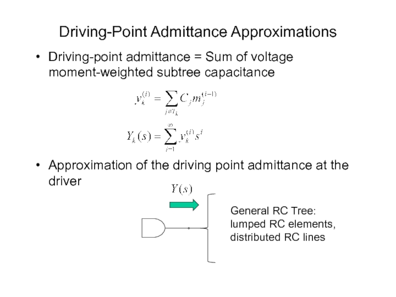
Driving-point admittance = Sum of voltage moment-weighted subtree capacitance
Approximation
General RC Tree:
lumped RC elements,
distributed RC lines
Слайд 43Driving-Point Admittance Approximations
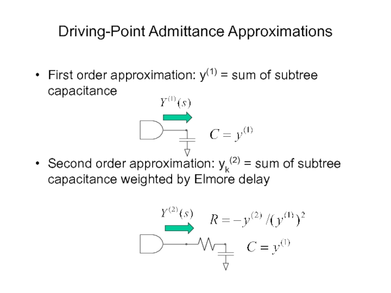
First order approximation: y(1) = sum of subtree capacitance
Second
Слайд 45Current Moment Computation
Similar to the voltage moment computation
Iterative tree traversal:
O(n) run-time,
Bottom-up tree traversal:
O(n) run-time
Can achieve O(k) storage if we impose order of traversal, k = max degree of a node
O’Brian and Savarino used bottom-up tree traversal
Слайд 46Bottom-Up Moment Computation
Maintain transfer function Hv~w(s) for sink w in subtree
As we merge subtrees, compute new transfer function Hu~v(s) and weighted capacitance recursively:
New transfer function for node w
New moment-weighted capacitance of Tu:
Слайд 51
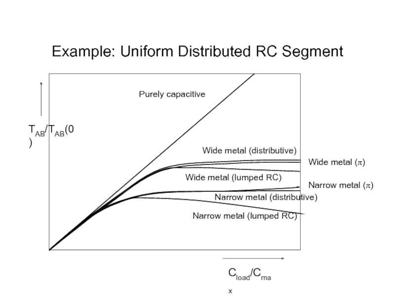
Example: Uniform Distributed RC Segment
Purely capacitive
Wide metal (distributive)
Narrow metal (distributive)
Narrow metal
Wide metal (lumped RC)
Wide metal (π)
Narrow metal (π)
Cload/Cmax
TAB/TAB(0)
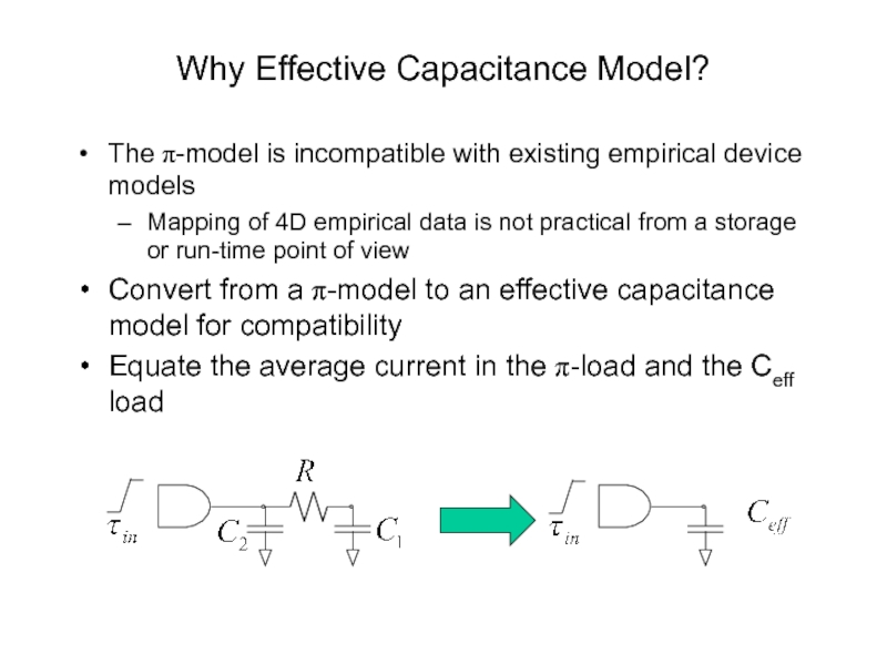
Слайд 52Why Effective Capacitance Model?
The π-model is incompatible with existing empirical device
Mapping of 4D empirical data is not practical from a storage or run-time point of view
Convert from a π-model to an effective capacitance model for compatibility
Equate the average current in the π-load and the Ceff load
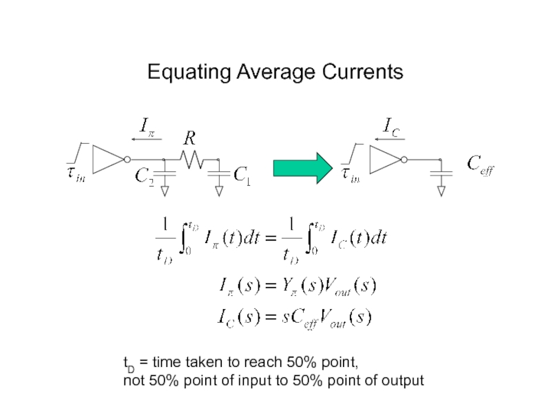
Слайд 53Equating Average Currents
tD = time taken to reach 50% point,
not
Слайд 54Waveform Approximation for Vout(t)
Quadratic from initial voltage (Vi = VDD for
Voltage waveform and first derivative are continuous at tx
Слайд 55Average Currents in Capacitors
Average current of C1 is not quite as
Current due to quadratic current in C2
Current due to linear current in C2
Слайд 56Average current for (0,tx) in C2
Average current for (tx,tD) in C2
Average
Average Currents in C1
Слайд 57Computation of Effective Capacitance
Equating average currents
Problem: tD and tx are not
Solution: iterative computation
Set the load capacitance equal to total capacitance
Use table-lookup or K-factor equations to obtain tD and tx
Equate average currents and calculate effective capacitance
Set load capacitance equal to effective capacitance and iterate
Слайд 58 Stage Delay Computation
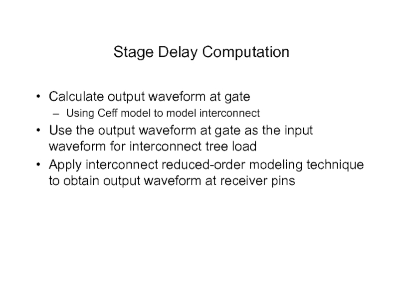
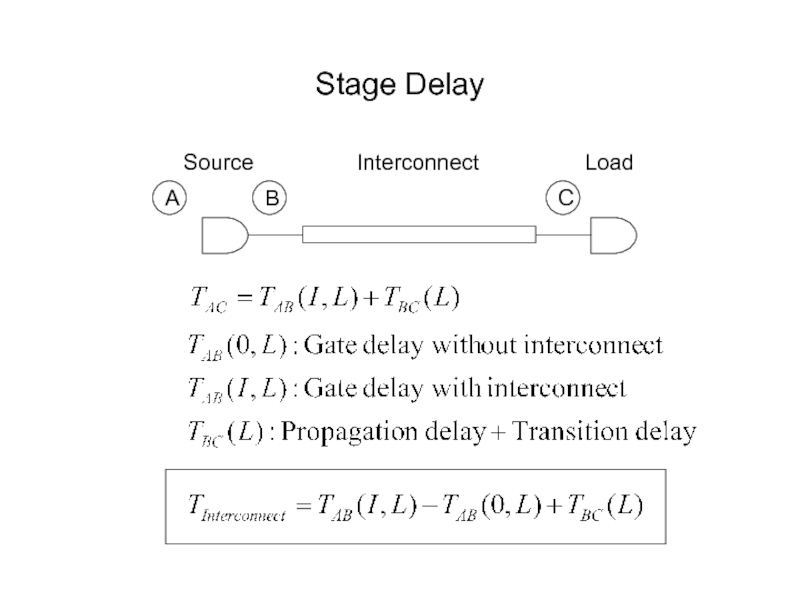
Calculate output waveform at gate
Using Ceff model to
Use the output waveform at gate as the input waveform for interconnect tree load
Apply interconnect reduced-order modeling technique to obtain output waveform at receiver pins

![Elmore Delay of a RC Tree [Rubinstein-Penfield-Horowitz, T-CAD’83]Lemma:Proof:Apply impulse func. at t=0:iminicurrent i→imin](/img/tmb/5/483238/94ab43296cddd3b9b1d158bb38c9b564-800x.jpg)
![Π-Model [O’Brian-Savarino, ICCAD’89]Moment matching again!Consider the first three moments of driving point admittance (moments of](/img/tmb/5/483238/30474638231eb2a4eb1285bc47f4793d-800x.jpg)
