- Главная
- Разное
- Дизайн
- Бизнес и предпринимательство
- Аналитика
- Образование
- Развлечения
- Красота и здоровье
- Финансы
- Государство
- Путешествия
- Спорт
- Недвижимость
- Армия
- Графика
- Культурология
- Еда и кулинария
- Лингвистика
- Английский язык
- Астрономия
- Алгебра
- Биология
- География
- Детские презентации
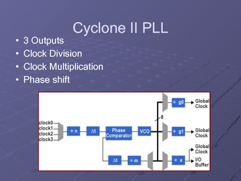
- Информатика
- История
- Литература
- Маркетинг
- Математика
- Медицина
- Менеджмент
- Музыка
- МХК
- Немецкий язык
- ОБЖ
- Обществознание
- Окружающий мир
- Педагогика
- Русский язык
- Технология
- Физика
- Философия
- Химия
- Шаблоны, картинки для презентаций
- Экология
- Экономика
- Юриспруденция
Programmable Logic and FPGA презентация
Содержание
- 1. Programmable Logic and FPGA
- 2. Objectives What is a programmable logic What
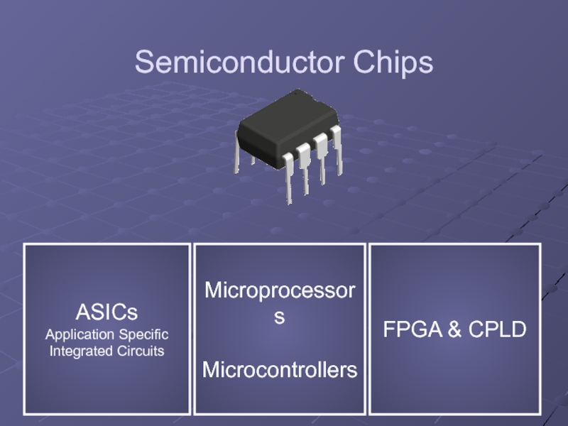
- 3. Semiconductor Chips FPGA & CPLD ASICs Application Specific Integrated Circuits Microprocessors Microcontrollers
- 4. Programmable logic An integrated circuit that can
- 5. Advantages Short Development time Reconfigurable Saves board
- 6. How it Began : PLA Programmable Logic
- 7. SPLD - CPLD Simple Programmable logic device
- 8. FPGA - Field Programmable Gate Array Programmable
- 9. Configuring LUT Required Function Truth Table Programmed
- 10. Special FPGA functions Internal SRAM Embedded Multipliers
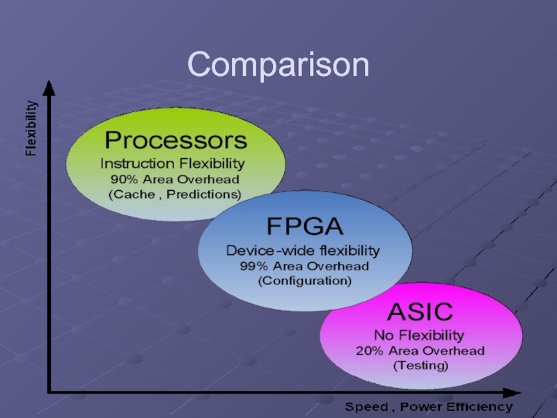
- 11. Comparison
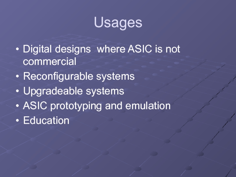
- 12. Usages Digital designs where ASIC is not
- 13. Manufacturers Xilinx Altera Lattice Actel We will work with Altera FPGAs
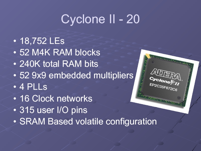
- 14. Cyclone II - 20 18,752 LEs
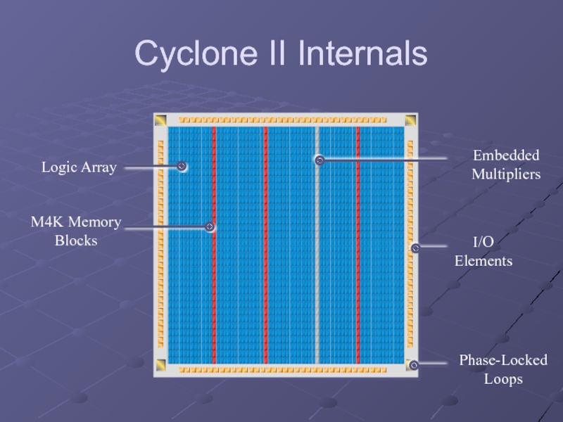
- 15. Cyclone II Internals
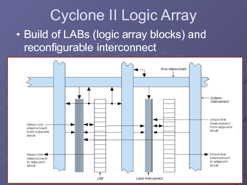
- 16. Cyclone II Logic Array Build of LABs (logic array blocks) and reconfigurable interconnect
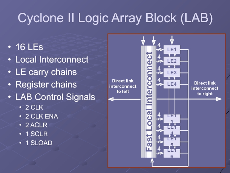
- 17. Cyclone II Logic Array Block (LAB) 16
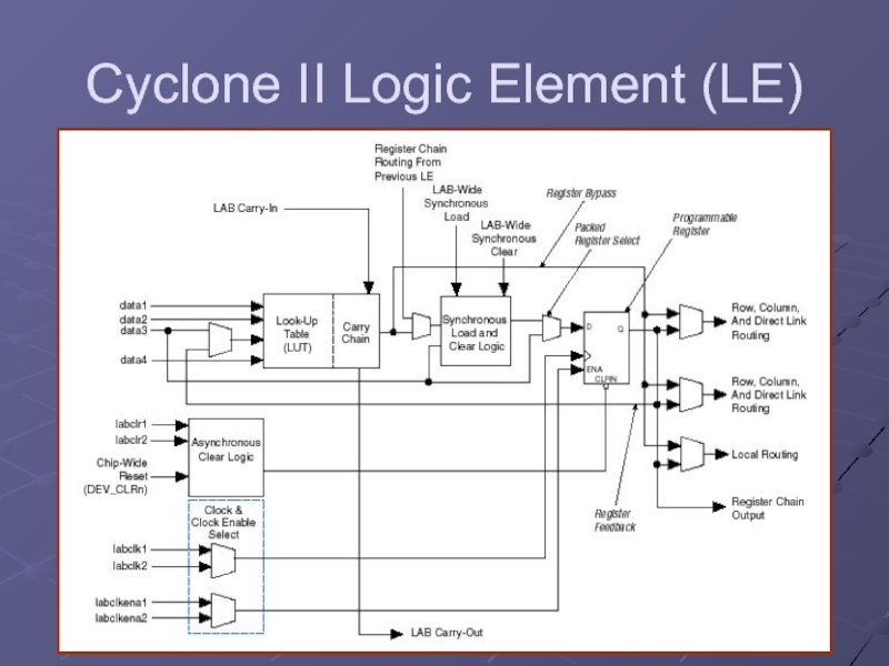
- 18. Cyclone II Logic Element (LE)
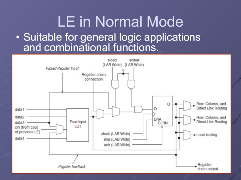
- 19. LE in Normal Mode Suitable for general logic applications and combinational functions.
- 20. LE in Arithmetic Mode Ideal for implementing adders, counters, accumulators, and comparators.
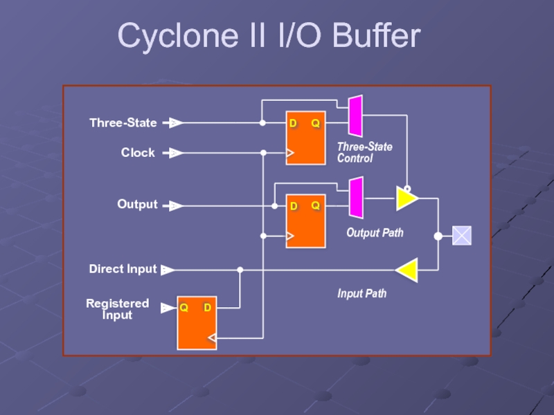
- 21. Cyclone II I/O Features In/Out/Tri-state Different Voltages
- 22. Cyclone II I/O Buffer
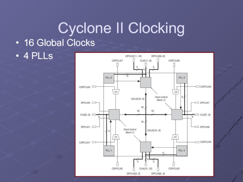
- 23. Cyclone II Clocking 16 Global Clocks 4 PLLs
- 24. Cyclone II PLL 3 Outputs Clock Division Clock Multiplication Phase shift
- 25. Memory True Dual port RAM/ROM with dual
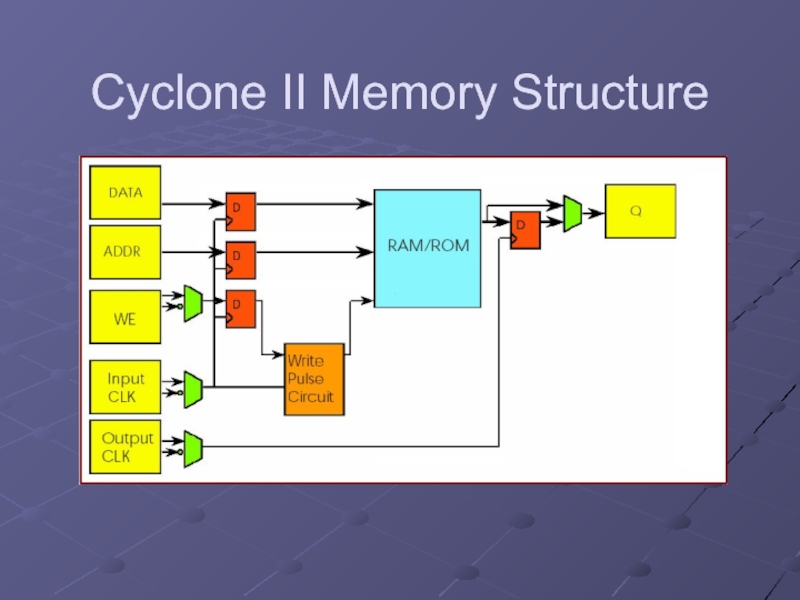
- 26. Cyclone II Memory Structure
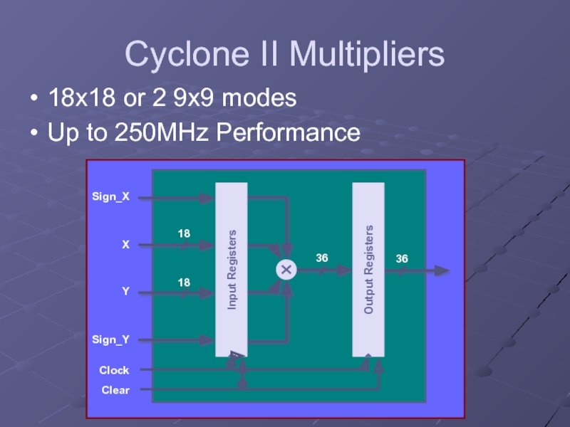
- 27. Cyclone II Multipliers 18x18 or 2 9x9 modes Up to 250MHz Performance
- 28. Delays and maximal frequency Gate delay –
- 29. Design flow
- 30. Design Rules
- 31. Any questions?
Слайд 2Objectives
What is a programmable logic
What is an FPGA
Structure
Special functions
Comparison and Usages
Altera
Cyclone II 20 FPGA
Design Flow
Design Flow
Слайд 3Semiconductor Chips
FPGA & CPLD
ASICs
Application Specific
Integrated Circuits
Microprocessors
Microcontrollers
Слайд 4Programmable logic
An integrated circuit that can be programmed/reprogrammed with a digital
logic of a curtain level.
Started at late 70s and constantly growing
Now available of up to approximately 700K Flip-Flops in a single chip.
Started at late 70s and constantly growing
Now available of up to approximately 700K Flip-Flops in a single chip.
Слайд 5Advantages
Short Development time
Reconfigurable
Saves board space
Flexible to changes
No need for ASIC expensive
design and production
Fast time to market
Bugs can be fixed easily
Of the shelf solutions are available
Fast time to market
Bugs can be fixed easily
Of the shelf solutions are available
Слайд 6How it Began : PLA
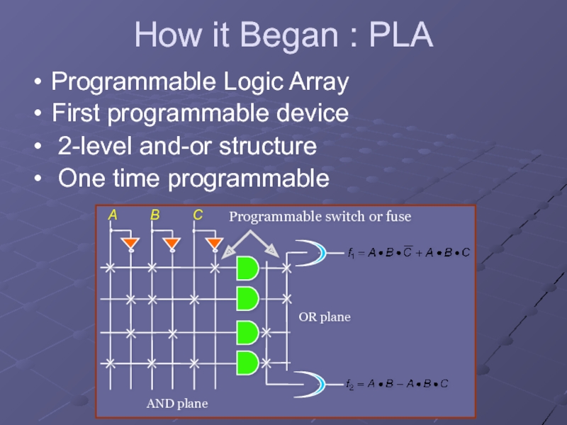
Programmable Logic Array
First programmable device
2-level and-or
structure
One time programmable
One time programmable
Слайд 7SPLD - CPLD
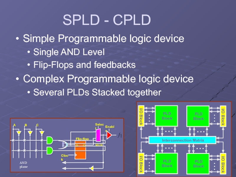
Simple Programmable logic device
Single AND Level
Flip-Flops and feedbacks
Complex Programmable
logic device
Several PLDs Stacked together
Several PLDs Stacked together
Слайд 8FPGA - Field Programmable Gate Array
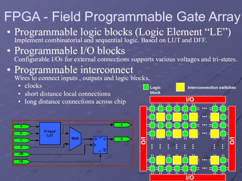
Programmable logic blocks (Logic Element “LE”)
Implement
combinatorial and sequential logic. Based on LUT and DFF.
Programmable I/O blocks Configurable I/Os for external connections supports various voltages and tri-states.
Programmable interconnect Wires to connect inputs , outputs and logic blocks.
clocks
short distance local connections
long distance connections across chip
Programmable I/O blocks Configurable I/Os for external connections supports various voltages and tri-states.
Programmable interconnect Wires to connect inputs , outputs and logic blocks.
clocks
short distance local connections
long distance connections across chip
Слайд 9Configuring LUT
Required Function
Truth Table
Programmed LUT
LUT is a RAM with data width
of 1bit.
The contents are programmed at power up
The contents are programmed at power up
Слайд 10Special FPGA functions
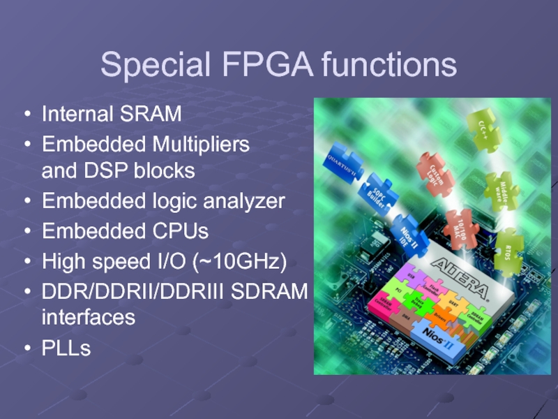
Internal SRAM
Embedded Multipliers
and DSP blocks
Embedded logic analyzer
Embedded CPUs
High
speed I/O (~10GHz)
DDR/DDRII/DDRIII SDRAM interfaces
PLLs
DDR/DDRII/DDRIII SDRAM interfaces
PLLs
Слайд 12Usages
Digital designs where ASIC is not commercial
Reconfigurable systems
Upgradeable systems
ASIC prototyping and
emulation
Education
Education
Слайд 14Cyclone II - 20
18,752 LEs
52 M4K RAM blocks
240K total
RAM bits
52 9x9 embedded multipliers
4 PLLs
16 Clock networks
315 user I/O pins
SRAM Based volatile configuration
52 9x9 embedded multipliers
4 PLLs
16 Clock networks
315 user I/O pins
SRAM Based volatile configuration
Слайд 15Cyclone II Internals
Logic Array
M4K Memory
Blocks
Embedded
Multipliers
Phase-Locked
Loops
I/O
Elements
Слайд 17Cyclone II Logic Array Block (LAB)
16 LEs
Local Interconnect
LE carry chains
Register chains
LAB
Control Signals
2 CLK
2 CLK ENA
2 ACLR
1 SCLR
1 SLOAD
2 CLK
2 CLK ENA
2 ACLR
1 SCLR
1 SLOAD
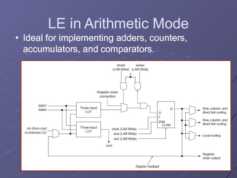
Слайд 20LE in Arithmetic Mode
Ideal for implementing adders, counters, accumulators, and comparators.
Слайд 21Cyclone II I/O Features
In/Out/Tri-state
Different Voltages and I/O Standards
Flip-flop option
Pull-up resistors
DDR interface
Series
resistors
Bus keeper
Drive strength control
Slew rate control
Single ended/differential
Bus keeper
Drive strength control
Slew rate control
Single ended/differential
Слайд 25Memory
True Dual port RAM/ROM with dual clock
Variable data width
4K×1, 2K×2,
1K×4, 512×8, 512×9, 256×16, 256×18
128×32, 128×36 (not available in true dual-port mode)
Input data and address are registered
1 Clock Write latency
Output data can be registered
Read latency of 1 or 2 clocks
Byte Enable
128×32, 128×36 (not available in true dual-port mode)
Input data and address are registered
1 Clock Write latency
Output data can be registered
Read latency of 1 or 2 clocks
Byte Enable
Слайд 28Delays and maximal frequency
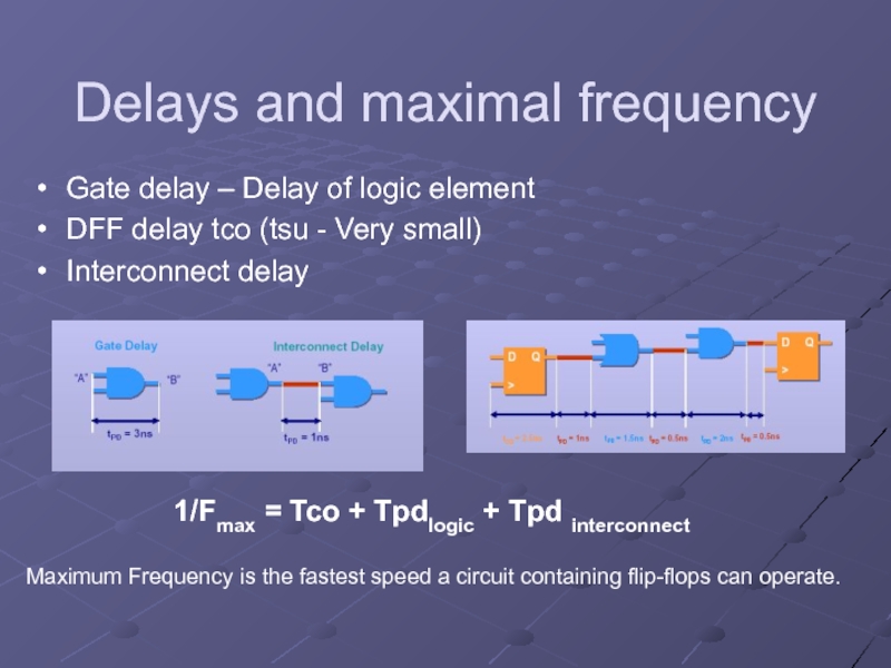
Gate delay – Delay of logic element
DFF
delay tco (tsu - Very small)
Interconnect delay
Interconnect delay
Maximum Frequency is the fastest speed a circuit containing flip-flops can operate.
1/Fmax = Tco + Tpdlogic + Tpd interconnect

