- Главная
- Разное
- Дизайн
- Бизнес и предпринимательство
- Аналитика
- Образование
- Развлечения
- Красота и здоровье
- Финансы
- Государство
- Путешествия
- Спорт
- Недвижимость
- Армия
- Графика
- Культурология
- Еда и кулинария
- Лингвистика
- Английский язык
- Астрономия
- Алгебра
- Биология
- География
- Детские презентации
- Информатика
- История
- Литература
- Маркетинг
- Математика
- Медицина
- Менеджмент
- Музыка
- МХК
- Немецкий язык
- ОБЖ
- Обществознание
- Окружающий мир
- Педагогика
- Русский язык
- Технология
- Физика
- Философия
- Химия
- Шаблоны, картинки для презентаций
- Экология
- Экономика
- Юриспруденция
Placement and routing guidelines for Power Electronics Devices презентация
Содержание
- 1. Placement and routing guidelines for Power Electronics Devices
- 2. Lecture plan Planning the layout. Single-board PCB
- 3. Current position: 1/7 Planning the layout. Single-board
- 4. PCB design for PE devices. Why is
- 5. Planning the layout. Each PE device contains
- 6. Planning the layout. Do we need to
- 7. Planning the layout.
- 8. Current position: 2/7 Planning the layout. Single-board
- 9. Single-board PCB layout. Power part location should
- 10. Single-board PCB layout. Typical PCB layout of the single-board PE device.
- 11. Single-board PCB layout. High speed components (both
- 12. Current position: 3/7 Planning the layout. Single-board
- 13. Stack of layers – 1, 2 or
- 14. Stack of layers – 1, 2 or
- 15. Stack of layers – 1, 2 or
- 16. Desirable stack of layers Typical stack of 4-layers PCB
- 17. Desirable stack of layers Typical stack of 6-layers PCB
- 18. Current position: 4/7 Planning the layout. Single-board
- 19. Important features of power part Highest currents
- 20. Buck Converter
- 21. Current loops ordered by EMI generation in
- 22. Boost converter
- 23. Transformer Isolated Flyback Converter
- 24. The first rule for PE devices PCB
- 25. PCB layout for buck converter. Red –
- 26. Red – rectifier loop, black – load loop. Output Rectifier Loop in Flyback Converter
- 27. Parallel C Filter Layout
- 28. Parallel C Filter Layout PCB layout between
- 29. Current position: 5/7 Planning the layout. Single-board
- 30. Grounding in the PE devices. Types of
- 31. Grounding in buck converter Red – control ground, blue – power ground.
- 32. Control and power ground connection. Rules of
- 33. Grounding in flyback converter
- 34. Current position: 6/7 Planning the layout. Single-board
- 35. Current sensor resistor PCB layout consideration The
- 36. Current sensor resistor PCB layout consideration Sensing trace
- 37. Land Patterns for SMD components in PE
- 38. Land Patterns for SMD components in PE devices Examples of Pad configuration:
- 39. Current position: 7/7 Planning the layout. Single-board
- 40. Mixed-signal grounding Mixed-signal components: External DAC and
- 41. Mixed-signal grounding Mixed-signal components: External DAC and
- 42. Digital and Analog Ground Bed design: Digital
- 43. Digital and Analog Ground Good design: Digital and analog ground are separated.
- 44. Digital and Analog Ground Planes for ground
- 45. Mixed-signal grounding – single PCB “Star”
- 46. Mixed-signal grounding – single PCB “Star”
- 47. Mixed-signal grounding – multi-board PCB Grounding
- 48. Mixed-signal grounding Small digital currents:
- 49. Mixed-signal grounding Small digital currents: http://www.analog.com/en/content/mixed_signal_dsp_design_book/fca.html
- 50. Mixed-signal grounding High digital currents: http://www.analog.com/en/content/mixed_signal_dsp_design_book/fca.html
- 51. Bypass Capacitors Noise on power line caused
- 52. Bypass Capacitors Bypass capacitor should be connected
- 53. Oscillator Layout Consideration Oscillator Circuit in common
Слайд 1Placement and routing guidelines for Power Electronics Devices
Printed Circuit Board
Dr. Oleksandr Velihorskyi, PhD
Слайд 2Lecture plan
Planning the layout.
Single-board PCB layout.
Placement of Layers for PE devices.
Current
Grounding in the PE devices.
Land Patterns for SMD components in PE devices.
Control scheme layout consideration.
Слайд 3Current position: 1/7
Planning the layout.
Single-board PCB layout.
Placement of Layers for PE
Current loops in Power Electronics Devices.
Grounding in the PE devices.
Land Patterns for SMD components in PE devices.
Control scheme layout consideration.
Слайд 4PCB design for PE devices. Why is it so important?
Improper PCB
"unstable" switching waveforms and jittering,
audible noise from the magnetic components,
ringing, crosstalk, ground bounce,
PCB design can lead good scheme to fail.
but even best PCB design can’t improve bad schematic solution.
Слайд 5Planning the layout.
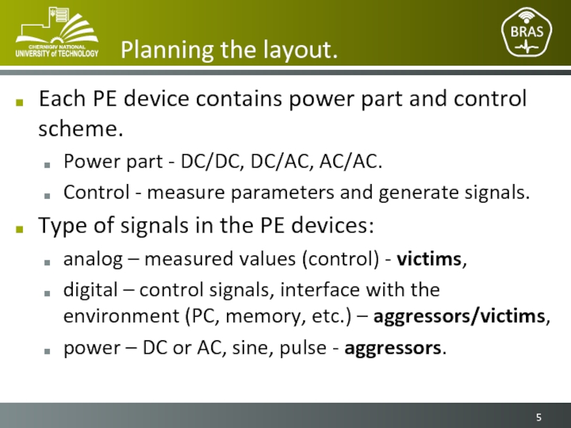
Each PE device contains power part and control scheme.
Power
Control - measure parameters and generate signals.
Type of signals in the PE devices:
analog – measured values (control) - victims,
digital – control signals, interface with the environment (PC, memory, etc.) – aggressors/victims,
power – DC or AC, sine, pulse - aggressors.
Слайд 6Planning the layout.
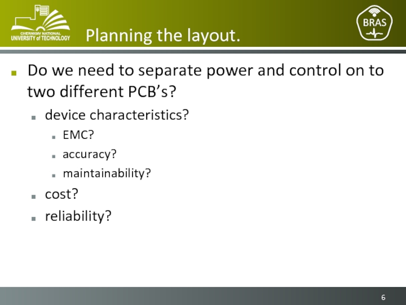
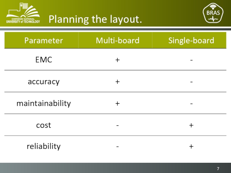
Do we need to separate power and control on
device characteristics?
EMC?
accuracy?
maintainability?
cost?
reliability?
Слайд 8Current position: 2/7
Planning the layout.
Single-board PCB layout.
Placement of Layers for PE
Current loops in Power Electronics Devices.
Grounding in the PE devices.
Land Patterns for SMD components in PE devices.
Control scheme layout consideration.
Слайд 9Single-board PCB layout.
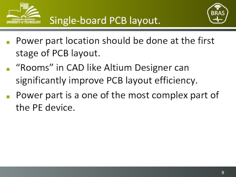
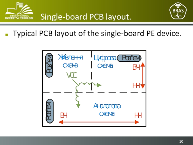
Power part location should be done at the first
“Rooms” in CAD like Altium Designer can significantly improve PCB layout efficiency.
Power part is a one of the most complex part of the PE device.
Слайд 11Single-board PCB layout.
High speed components (both analog and digital) need to
Analog and digital signals in an ideal case should never run parallel to each other at a small distance!
Слайд 12Current position: 3/7
Planning the layout.
Single-board PCB layout.
Placement of Layers for PE
Current loops in Power Electronics Devices.
Grounding in the PE devices.
Land Patterns for SMD components in PE devices.
Control scheme layout consideration.
Слайд 13Stack of layers – 1, 2 or more?
1-layer PCB:
Most sensitive to
Need to use Jumpers.
2-layer PCB:
Better than 1-layer – more space for traces/components.
More resistant to EMI.
Plane layers are possible, but not fully realizable.
BGA components is not eligible.
Слайд 14Stack of layers – 1, 2 or more?
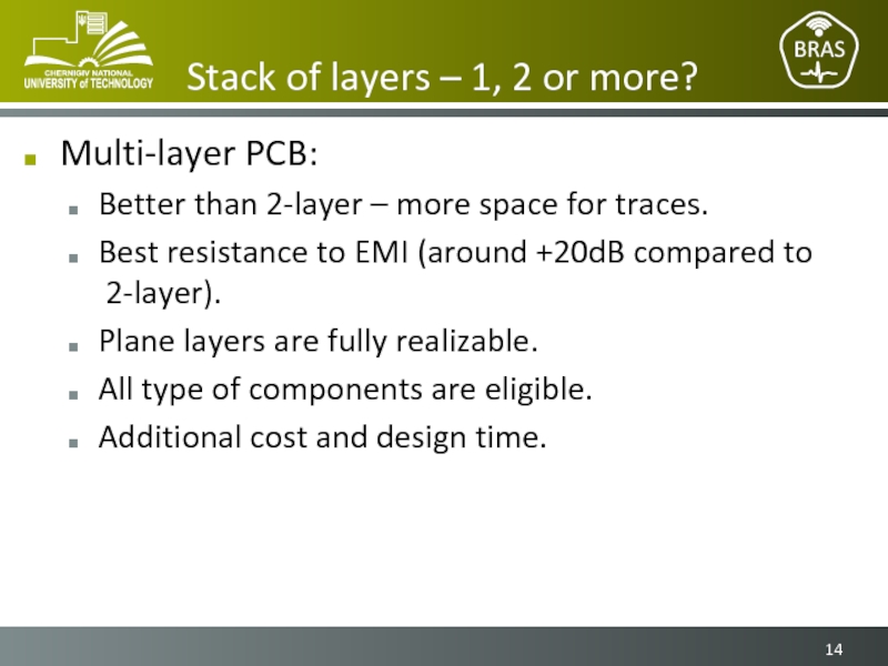
Multi-layer PCB:
Better than 2-layer
Best resistance to EMI (around +20dB compared to 2-layer).
Plane layers are fully realizable.
All type of components are eligible.
Additional cost and design time.
Слайд 15Stack of layers – 1, 2 or more?
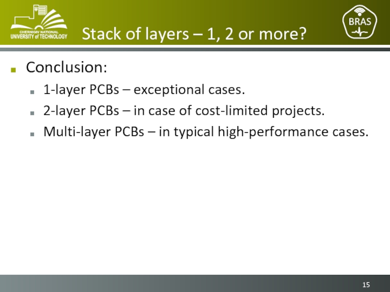
Conclusion:
1-layer PCBs – exceptional
2-layer PCBs – in case of cost-limited projects.
Multi-layer PCBs – in typical high-performance cases.
Слайд 18Current position: 4/7
Planning the layout.
Single-board PCB layout.
Placement of Layers for PE
Current loops in Power Electronics Devices.
Grounding in the PE devices.
Land Patterns for SMD components in PE devices.
Control scheme layout consideration.
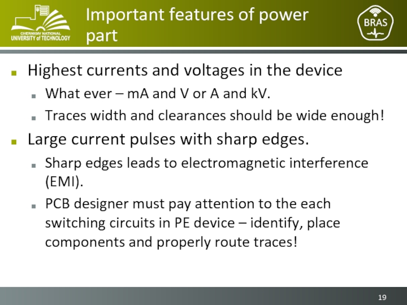
Слайд 19Important features of power part
Highest currents and voltages in the device
What
Traces width and clearances should be wide enough!
Large current pulses with sharp edges.
Sharp edges leads to electromagnetic interference (EMI).
PCB designer must pay attention to the each switching circuits in PE device – identify, place components and properly route traces!
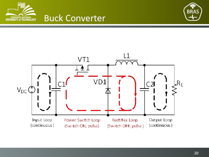
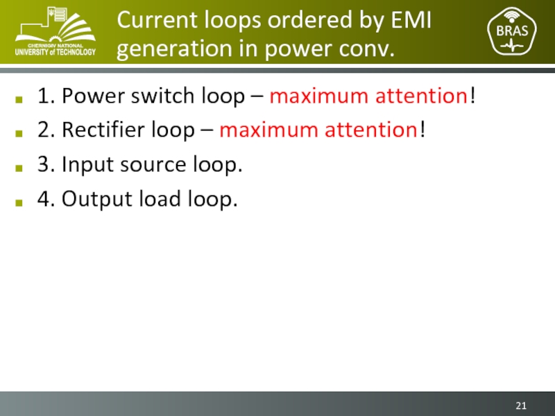
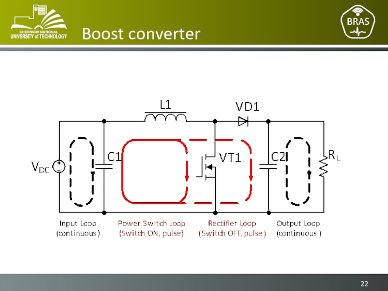
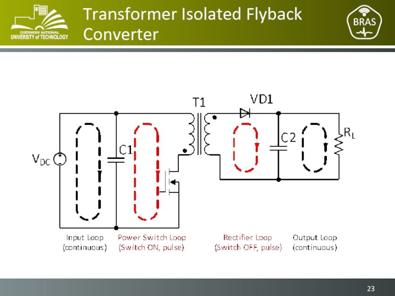
Слайд 21Current loops ordered by EMI generation in power conv.
1. Power switch
2. Rectifier loop – maximum attention!
3. Input source loop.
4. Output load loop.
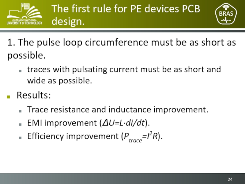
Слайд 24The first rule for PE devices PCB design.
1. The pulse loop
traces with pulsating current must be as short and wide as possible.
Results:
Trace resistance and inductance improvement.
EMI improvement (ΔU=L·di/dt).
Efficiency improvement (Ptrace=I2R).
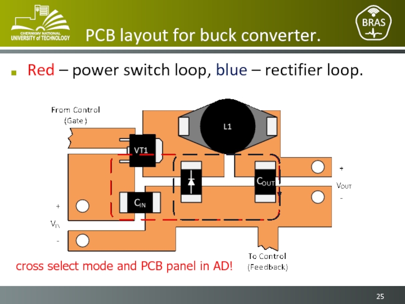
Слайд 25PCB layout for buck converter.
Red – power switch loop, blue –
cross select mode and PCB panel in AD!
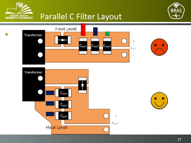
Слайд 28Parallel C Filter Layout
PCB layout between each capacitor and source in
Non-identical layout will lead to different current sharing and will reduce capacitor lifespan (mean time between failures, MTBF).
Слайд 29Current position: 5/7
Planning the layout.
Single-board PCB layout.
Placement of Layers for PE
Current loops in Power Electronics Devices.
Grounding in the PE devices.
Land Patterns for SMD components in PE devices.
Control scheme layout consideration.
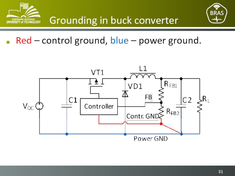
Слайд 30Grounding in the PE devices.
Types of ground in power convertor devices:
Power
Signal ground in controller and feedback part.
Analog ground for feedback.
Digital ground for controller (MCU, DSP or FPGA device).
Main rule: “separate ground for high-current and signal part”!
Слайд 32Control and power ground connection.
Rules of thumb for grounding in PE
Feedback ground must be connected with power ground near the negative pin of output capacitor.
If control IC has separated (power and control) ground, these pins must be routed separately and connected to the current sensing resistor that measure power switch current.
Слайд 34Current position: 6/7
Planning the layout.
Single-board PCB layout.
Placement of Layers for PE
Current loops in Power Electronics Devices.
Grounding in the PE devices.
Land Patterns for SMD components in PE devices.
Control scheme layout consideration.
Слайд 35Current sensor resistor PCB layout consideration
The best characteristic provides 4-wire Kelvin
Example of using 2-wire resistors as 4-wire Kelvin
Слайд 36Current sensor resistor PCB layout consideration
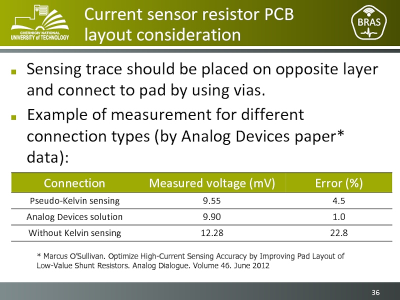
Sensing trace should be placed on opposite
Example of measurement for different connection types (by Analog Devices paper* data):
* Marcus O’Sullivan. Optimize High-Current Sensing Accuracy by Improving Pad Layout of Low-Value Shunt Resistors. Analog Dialogue. Volume 46. June 2012
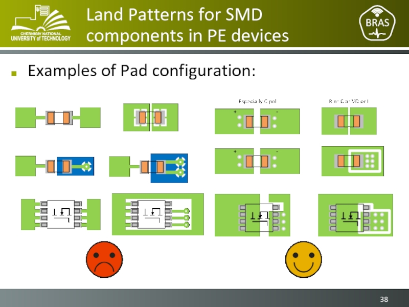
Слайд 37Land Patterns for SMD components in PE devices
For minimization of ESL
Without thermal connection.
With vias as close as possible to pad.
With sufficient number of vias in case of changing layer near the pad.
Notice:
SMD pad without thermal relief could cause soldering problem!
Слайд 39Current position: 7/7
Planning the layout.
Single-board PCB layout.
Placement of Layers for PE
Current loops in Power Electronics Devices.
Grounding in the PE devices.
Land Patterns for SMD components in PE devices.
Control scheme layout consideration.
Слайд 40Mixed-signal grounding
Mixed-signal components:
External DAC and ADC, MCU with DAC/ADC on board.
Ground
Digital?
Analog?
Some pins – digital, another ones – analog?
Слайд 41Mixed-signal grounding
Mixed-signal components:
External DAC and ADC, MCU with DAC/ADC on board.
Ground
Digital?
Analog?
Some pins – digital, another ones – analog?
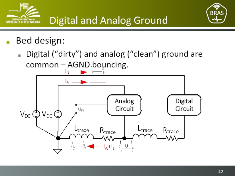
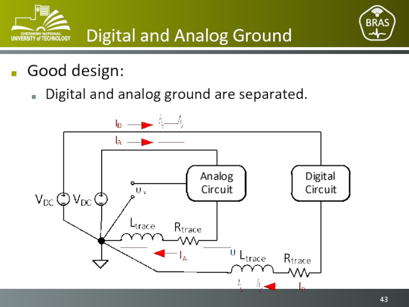
Слайд 42Digital and Analog Ground
Bed design:
Digital (“dirty”) and analog (“clean”) ground are
Слайд 44Digital and Analog Ground
Planes for ground in control circuits of power
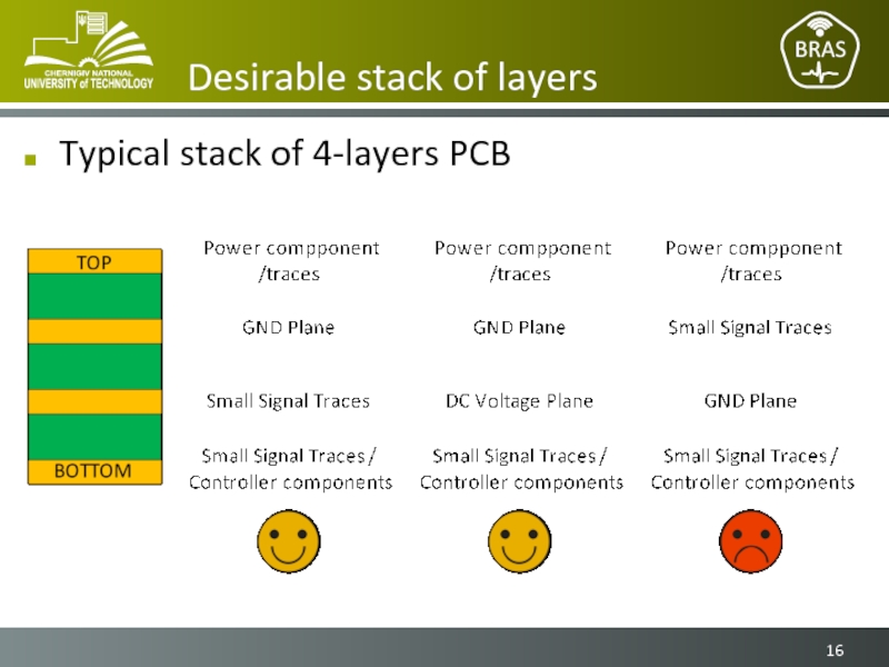
4-layer PCB (sig - VCC– GND - sig) is a typical solution for the control board.
VCC and GND planes provide additional distributed capacitance for control board power supply.
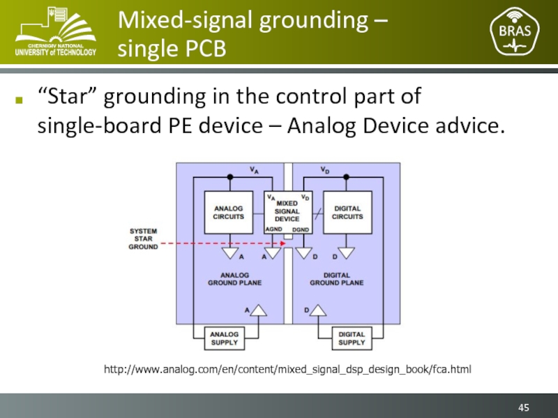
Слайд 45Mixed-signal grounding –
single PCB
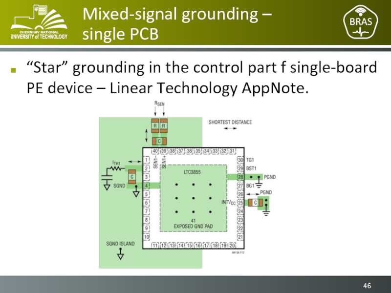
“Star” grounding in the control part of
http://www.analog.com/en/content/mixed_signal_dsp_design_book/fca.html
Слайд 46Mixed-signal grounding –
single PCB
“Star” grounding in the control part f
Слайд 47Mixed-signal grounding –
multi-board PCB
Grounding techniques for single-board PE devices are
Multi-board grounding techniques are depend on
Low digital currents.
High digital currents.
Provide additional ground pin in the connectors.
Recommend allocate 30-40% connector pins to GND.
Separate digital and analog signals by ground pins.
Слайд 49Mixed-signal grounding
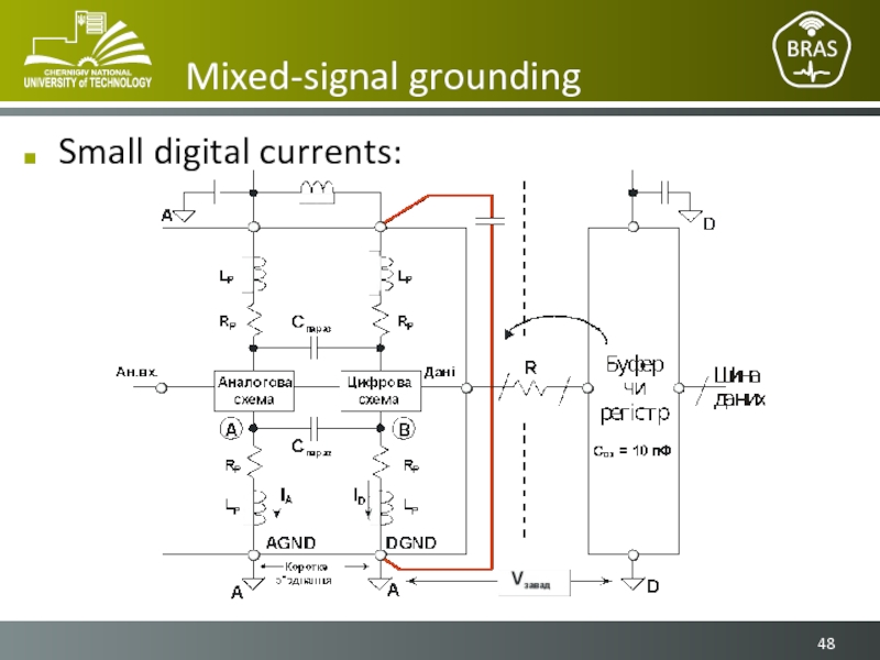
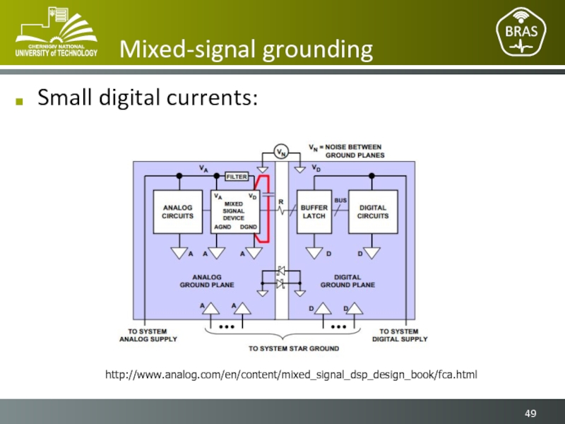
Small digital currents:
http://www.analog.com/en/content/mixed_signal_dsp_design_book/fca.html
Слайд 50Mixed-signal grounding
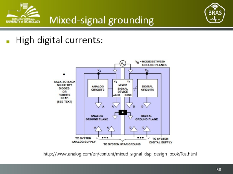
High digital currents:
http://www.analog.com/en/content/mixed_signal_dsp_design_book/fca.html
Слайд 51Bypass Capacitors
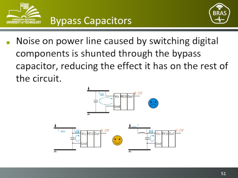
Noise on power line caused by switching digital components is
Слайд 52Bypass Capacitors
Bypass capacitor should be connected to the power pins of
Слайд 53Oscillator Layout Consideration
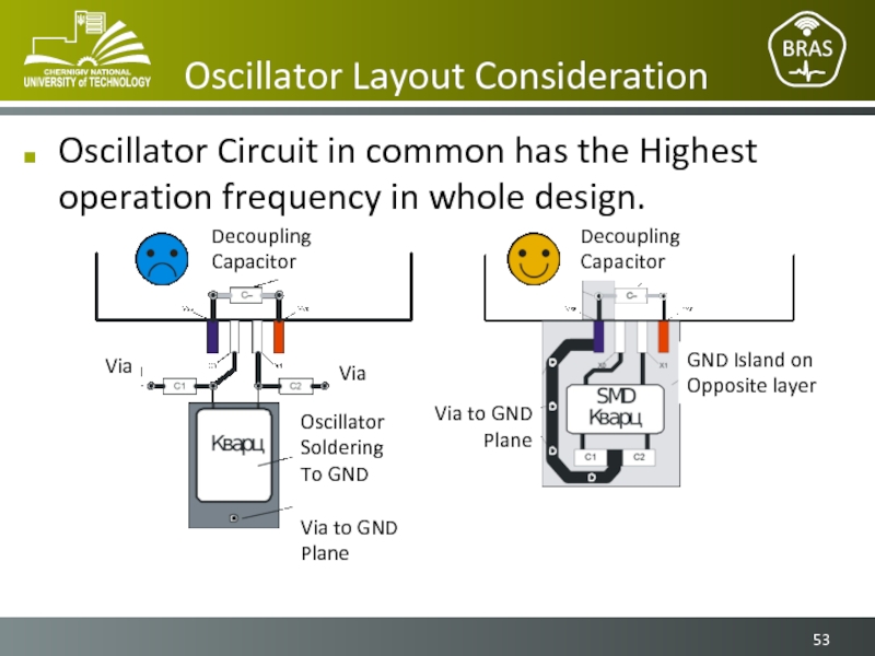
Oscillator Circuit in common has the Highest operation frequency
GND Island on
Opposite layer
Decoupling
Capacitor
Decoupling
Capacitor
Via
Via
Oscillator
Soldering
To GND
Via to GND Plane
Via to GND Plane
