- Главная
- Разное
- Дизайн
- Бизнес и предпринимательство
- Аналитика
- Образование
- Развлечения
- Красота и здоровье
- Финансы
- Государство
- Путешествия
- Спорт
- Недвижимость
- Армия
- Графика
- Культурология
- Еда и кулинария
- Лингвистика
- Английский язык
- Астрономия
- Алгебра
- Биология
- География
- Детские презентации
- Информатика
- История
- Литература
- Маркетинг
- Математика
- Медицина
- Менеджмент
- Музыка
- МХК
- Немецкий язык
- ОБЖ
- Обществознание
- Окружающий мир
- Педагогика
- Русский язык
- Технология
- Физика
- Философия
- Химия
- Шаблоны, картинки для презентаций
- Экология
- Экономика
- Юриспруденция
CPU How It Works презентация
Содержание
- 1. CPU How It Works
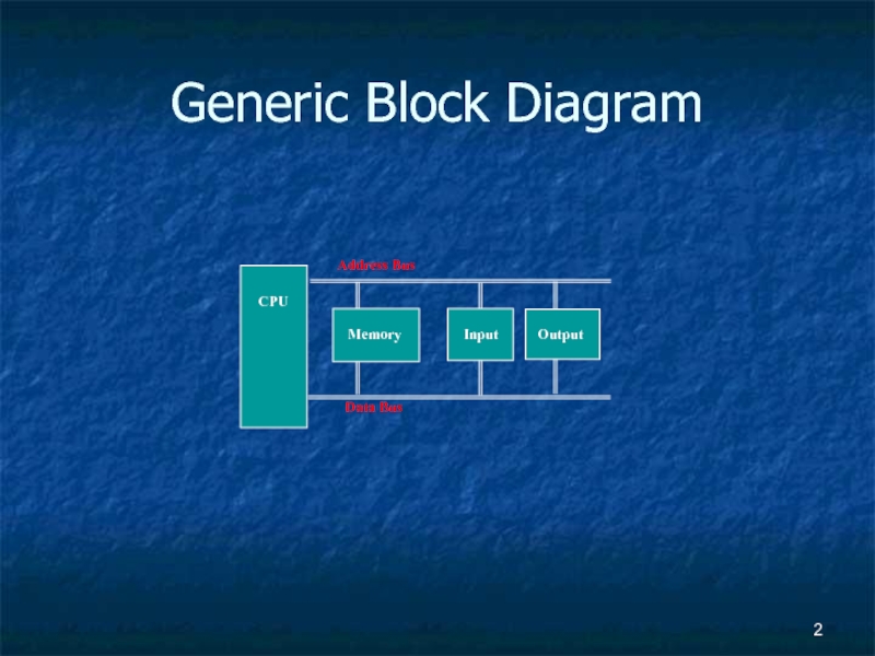
- 2. Generic Block Diagram CPU Memory Input Output Address Bus Data Bus
- 3. Hardware
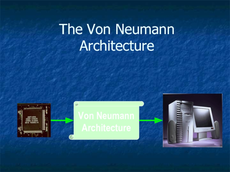
- 4. The Von Neumann Architecture Von Neumann Architecture
- 5. Designing Computers All computers more or less
- 6. The Von Neumann Architecture Model for designing
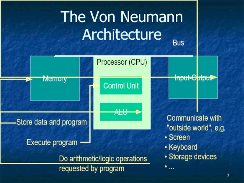
- 7. The Von Neumann Architecture Memory Processor (CPU) Input-Output Control Unit ALU Bus
- 8. Memory Subsystem Memory, also called RAM (Random
- 9. Memory Size / Speed Typical memory in
- 10. Operations on Memory Fetch (address): Fetch
- 11. Structure of the Memory Subsystem Fetch(address) Load
- 12. Input/Output Subsystem Handles devices that allow the
- 13. I/O Controllers Speed of I/O devices is
- 14. I/O controller Structure of the I/O
- 15. The ALU Subsystem The ALU (Arithmetic/Logic Unit)
- 16. Structure of the ALU Registers: Very
- 17. The Control Unit Program is stored in
- 18. Machine Language Instructions A machine language instruction
- 19. How does this all work together? Program
- 20. Program Execution (cont.) Fetch phase PC -->
- 21. Program Execution (cont.) Execute Phase Differs
Слайд 5Designing Computers
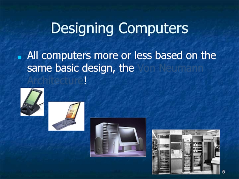
All computers more or less based on the same basic
Слайд 6The Von Neumann Architecture
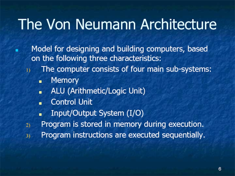
Model for designing and building computers, based on
The computer consists of four main sub-systems:
Memory
ALU (Arithmetic/Logic Unit)
Control Unit
Input/Output System (I/O)
Program is stored in memory during execution.
Program instructions are executed sequentially.
Слайд 8Memory Subsystem
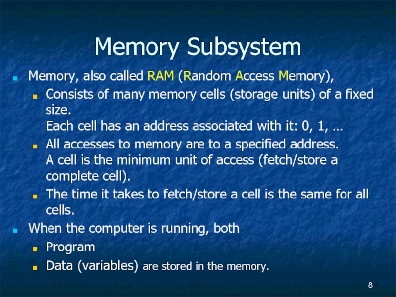
Memory, also called RAM (Random Access Memory),
Consists of many
All accesses to memory are to a specified address. A cell is the minimum unit of access (fetch/store a complete cell).
The time it takes to fetch/store a cell is the same for all cells.
When the computer is running, both
Program
Data (variables) are stored in the memory.
Слайд 9Memory Size / Speed
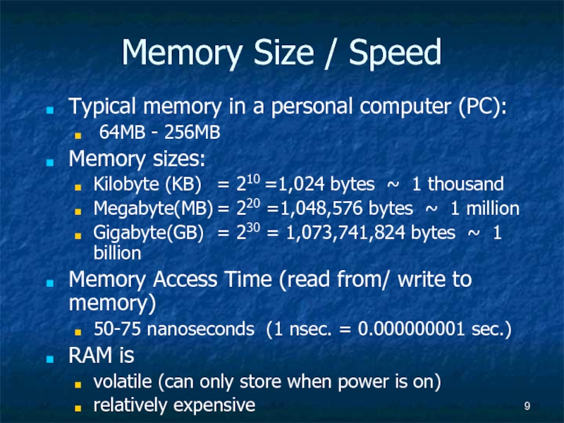
Typical memory in a personal computer (PC):
64MB
Memory sizes:
Kilobyte (KB) = 210 =1,024 bytes ~ 1 thousand
Megabyte(MB) = 220 =1,048,576 bytes ~ 1 million
Gigabyte(GB) = 230 = 1,073,741,824 bytes ~ 1 billion
Memory Access Time (read from/ write to memory)
50-75 nanoseconds (1 nsec. = 0.000000001 sec.)
RAM is
volatile (can only store when power is on)
relatively expensive
Слайд 10Operations on Memory
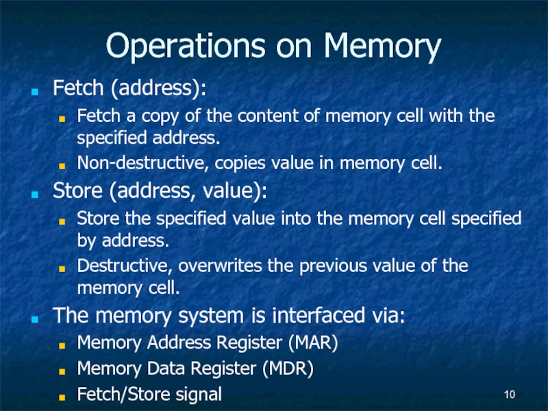
Fetch (address):
Fetch a copy of the content of
Non-destructive, copies value in memory cell.
Store (address, value):
Store the specified value into the memory cell specified by address.
Destructive, overwrites the previous value of the memory cell.
The memory system is interfaced via:
Memory Address Register (MAR)
Memory Data Register (MDR)
Fetch/Store signal
Слайд 11Structure of the Memory Subsystem
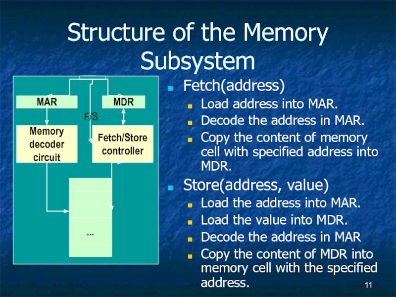
Fetch(address)
Load address into MAR.
Decode the address in
Copy the content of memory cell with specified address into MDR.
Store(address, value)
Load the address into MAR.
Load the value into MDR.
Decode the address in MAR
Copy the content of MDR into memory cell with the specified address.
MAR
MDR
...
Memory
decoder
circuit
Fetch/Store
controller
F/S
Слайд 12Input/Output Subsystem
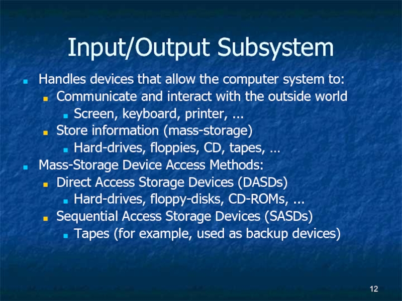
Handles devices that allow the computer system to:
Communicate and interact
Screen, keyboard, printer, ...
Store information (mass-storage)
Hard-drives, floppies, CD, tapes, …
Mass-Storage Device Access Methods:
Direct Access Storage Devices (DASDs)
Hard-drives, floppy-disks, CD-ROMs, ...
Sequential Access Storage Devices (SASDs)
Tapes (for example, used as backup devices)
Слайд 13I/O Controllers
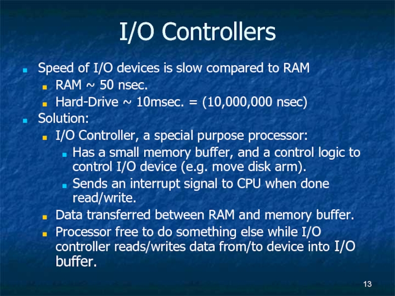
Speed of I/O devices is slow compared to RAM
RAM ~
Hard-Drive ~ 10msec. = (10,000,000 nsec)
Solution:
I/O Controller, a special purpose processor:
Has a small memory buffer, and a control logic to control I/O device (e.g. move disk arm).
Sends an interrupt signal to CPU when done read/write.
Data transferred between RAM and memory buffer.
Processor free to do something else while I/O controller reads/writes data from/to device into I/O buffer.
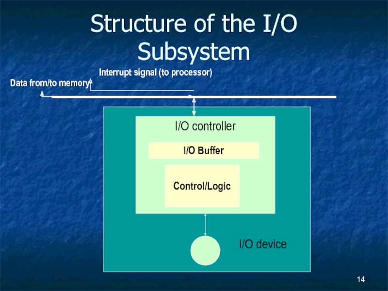
Слайд 14
I/O controller
Structure of the I/O Subsystem
I/O Buffer
Control/Logic
I/O device
Data from/to memory
Interrupt signal
Слайд 15The ALU Subsystem
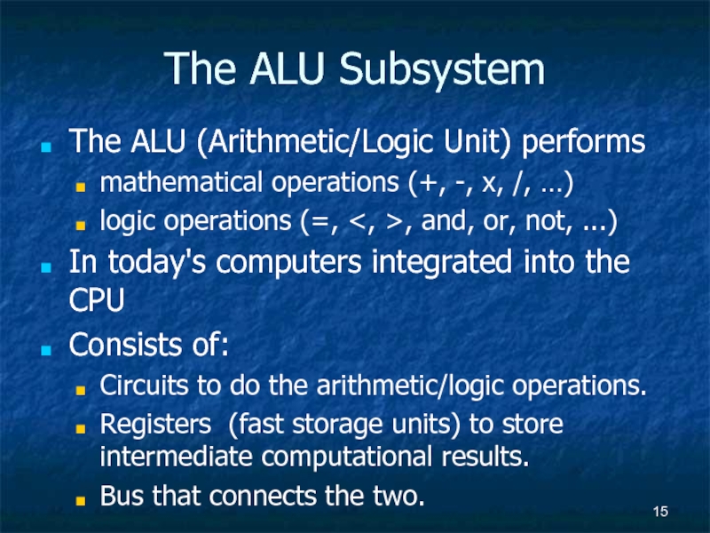
The ALU (Arithmetic/Logic Unit) performs
mathematical operations (+, -, x,
logic operations (=, <, >, and, or, not, ...)
In today's computers integrated into the CPU
Consists of:
Circuits to do the arithmetic/logic operations.
Registers (fast storage units) to store intermediate computational results.
Bus that connects the two.
Слайд 16
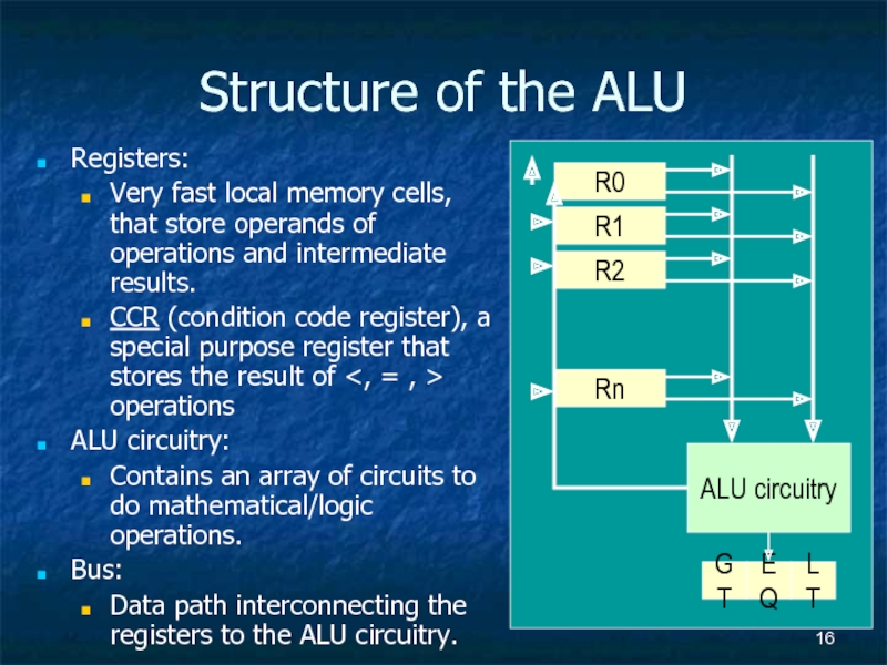
Structure of the ALU
Registers:
Very fast local memory cells, that store operands
CCR (condition code register), a special purpose register that stores the result of <, = , > operations
ALU circuitry:
Contains an array of circuits to do mathematical/logic operations.
Bus:
Data path interconnecting the registers to the ALU circuitry.
ALU circuitry
R0
R1
R2
Rn
Слайд 17The Control Unit
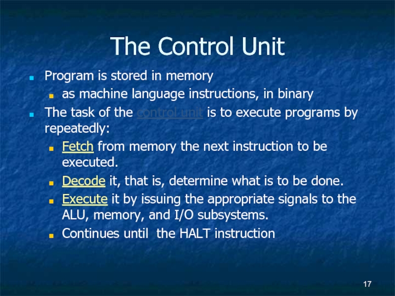
Program is stored in memory
as machine language instructions,
The task of the control unit is to execute programs by repeatedly:
Fetch from memory the next instruction to be executed.
Decode it, that is, determine what is to be done.
Execute it by issuing the appropriate signals to the ALU, memory, and I/O subsystems.
Continues until the HALT instruction
Слайд 18Machine Language Instructions
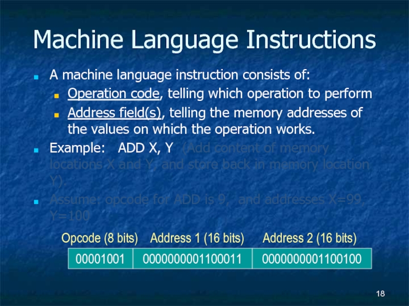
A machine language instruction consists of:
Operation code, telling which
Address field(s), telling the memory addresses of the values on which the operation works.
Example: ADD X, Y (Add content of memory locations X and Y, and store back in memory location Y).
Assume: opcode for ADD is 9, and addresses X=99, Y=100
00001001
0000000001100011
0000000001100100
Opcode (8 bits)
Address 1 (16 bits)
Address 2 (16 bits)
Слайд 19How does this all work together?
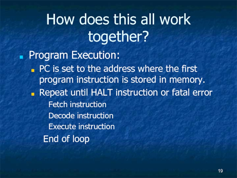
Program Execution:
PC is set to the
Repeat until HALT instruction or fatal error
Fetch instruction
Decode instruction
Execute instruction
End of loop
Слайд 20Program Execution (cont.)
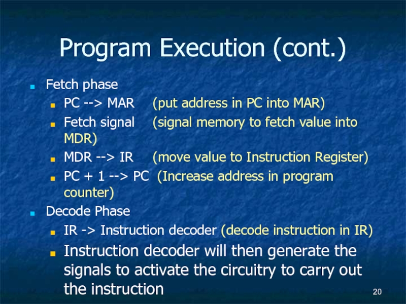
Fetch phase
PC --> MAR (put address in PC into MAR)
Fetch
MDR --> IR (move value to Instruction Register)
PC + 1 --> PC (Increase address in program counter)
Decode Phase
IR -> Instruction decoder (decode instruction in IR)
Instruction decoder will then generate the signals to activate the circuitry to carry out the instruction
Слайд 21Program Execution (cont.)
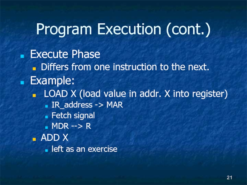
Execute Phase
Differs from one instruction to the next.
Example:
IR_address -> MAR
Fetch signal
MDR --> R
ADD X
left as an exercise
