- Главная
- Разное
- Дизайн
- Бизнес и предпринимательство
- Аналитика
- Образование
- Развлечения
- Красота и здоровье
- Финансы
- Государство
- Путешествия
- Спорт
- Недвижимость
- Армия
- Графика
- Культурология
- Еда и кулинария
- Лингвистика
- Английский язык
- Астрономия
- Алгебра
- Биология
- География
- Детские презентации
- Информатика
- История
- Литература
- Маркетинг
- Математика
- Медицина
- Менеджмент
- Музыка
- МХК
- Немецкий язык
- ОБЖ
- Обществознание
- Окружающий мир
- Педагогика
- Русский язык
- Технология
- Физика
- Философия
- Химия
- Шаблоны, картинки для презентаций
- Экология
- Экономика
- Юриспруденция
2012 Component Training Ivy Platform Series презентация
Содержание
- 1. 2012 Component Training Ivy Platform Series
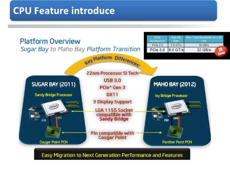
- 2. Platform Structure CPU feature introduce Intel 7
- 8. Platform Structure CPU feature introduce Intel 7
- 11. Platform Structure CPU feature introduce Intel 7
- 12. 7 Series due to over clocking, Z77&H77
- 14. 1. If PCH internal provide CLK, it
- 15. To 14M_PCH Check
- 16. Platform Structure CPU feature introduce Intel 7
- 17. SIO 3V_ATX +BAT_3V SR107 S_DSWVRMEN Power
- 18. SIO Power Button O_PWRBTN#IN O_PWRBTN# SIO SLP_S3#
- 20. Platform Structure CPU feature introduce Intel 7
- 21. +3VSB_ATX +3VSB_ATX PWRBTN# PANEL (B)
- 22. 2. Check PCH power sequence and working
- 23. 4. O_SKTOCC: SIO uses this pin to
- 24. Update BIOS or exchange another BIOS chipset
- 25. +3VSB_ATX +3VSB_ATX PWRBTN# PANEL (B)
- 26. If PCH working condition is abnormal, MB
- 27. Problem with power shutdown: THERMAL signals, voltage,
- 28. After 00 and CPURST#: CPU to PCH
- 29. Measure BUS: DMI: H_DMI_RXN/P[0:3] H_DMI_TXN/P[0:3] S_DMICOMP S_DMIRBIAS
- 30. LPC SMBUS CLOCK PWM ADC FAN
- 31. Refer model: P8Z77-V LE
- 32. Refer model: P8Z77-V LE
- 33. Measure CPU voltage: VCORE, GFX, VCCIO, VCCSA,
- 34. FDI and DMI Bus, make sure that
- 35. Vcc=3.3V Vinsen = 0.86V VRHot = Vcc
- 36. Vcc= 5V DVD= 1.5V≧1.11 DVDA = 1.33V≧1.11
- 37. Vcc5= 5V Vcc12= 12V EN=VCCIO≒ 1.05V
- 38. ASP0A13
- 39. IR8510
- 40. Vcore voltage output of each phase must
- 41. If you suspect that other components are
- 42. high low Clear COMS and
- 43. 5VSB P_3VSB_VDD_10 P_3VSB_PVDD_S P_+3VSB_RT_10 P_3VSB_R_FB_10 3VSB 0 ohm
- 44. high low low low high low
- 45. 5VDUAL and PU501 VCC Check P_1V5DUAL_OCSET/EN_10 Check
- 46. 8.2K ohm 25.5 K ohm Low
- 47. 3VSB 3VSB 10K
- 48. Thank You!

Слайд 2Platform Structure
CPU feature introduce
Intel 7 series chipset architecture
Critical Power Flow
Clock Distribution
Power
Problem Debug
Can’t power on
Power auto shutdown
All dots, zero, and no display
Power part

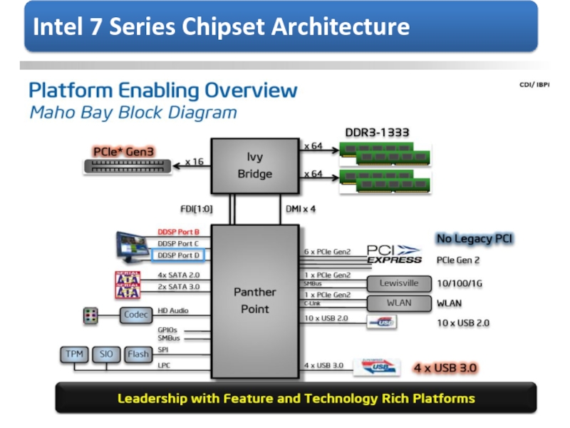
Слайд 8Platform Structure
CPU feature introduce
Intel 7 series chipset architecture
Critical Power Flow
Clock Distribution
Power
Problem Debug
Can’t power on
Power auto shutdown
All dots, zero, and no display
Power part

Слайд 11Platform Structure
CPU feature introduce
Intel 7 series chipset architecture
Critical Power Flow
Clock Distribution
Power
Problem Debug
Can’t power on
Power auto shutdown
All dots, zero, and no display
Power part

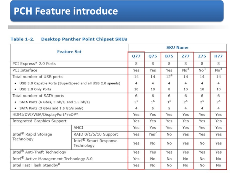
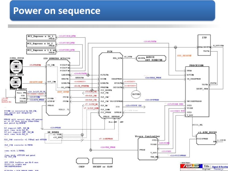
Слайд 127 Series due to over clocking, Z77&H77 series MB have some
Z77 series MB all use PCH integrate CLK GEN.
H77 series MB usually use external CLK GEN.


Слайд 14 1. If PCH internal provide CLK, it will use two 10K
2. If not, external CLK generator will provide 100M Hz frequency for PCH


Слайд 16Platform Structure
CPU feature introduce
Intel 7 series chipset architecture
Critical Power Flow
Clock Distribution
Power
Problem Debug
Can’t power on
Power auto shutdown
All dots, zero, and no display
Power part

Слайд 17SIO
3V_ATX
+BAT_3V
SR107
S_DSWVRMEN
Power Supply
S_RTCRST#
O_RSMRST#
O2_RSMRST#
1
2
3
4
6
SR106
S_INTVRMEN
SR79
S_SRTCRST#
SR75
S_RTCRST#
5
S_RTCRST #
O2_RSMRST#
P_+VTTCCIO_REF_10
P_+1.8SFR_REF_10
P_+VCCSA_REF_10
O_RSMRST#
O2_CUT_PSON#
O_PSON#
O2_PSON#
8
6
7
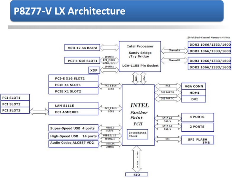
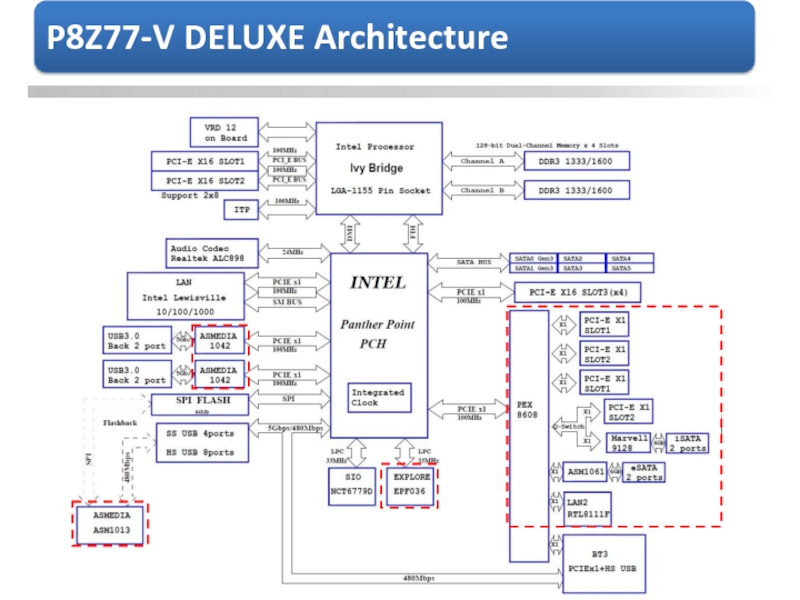
Refer model: P8Z77-V DELUXE

Слайд 18SIO
Power Button
O_PWRBTN#IN
O_PWRBTN#
SIO
SLP_S3#
SLP_S4#
O_PSON#
O2_CUT_PSON#
O2_PSON#
Power Supply
O2_PSON#
3V, 5V, 12V
Power Supply
B_ATX_PWROK
SIO
10
9
11
12
13
13
14
15

Слайд 20Platform Structure
CPU feature introduce
Intel 7 series chipset architecture
Critical Power Flow
Clock Distribution
Power
Problem Debug
Can’t power on
Power auto shutdown
All dots, zero, and no display
Power part

Слайд 21
+3VSB_ATX
+3VSB_ATX
PWRBTN#
PANEL (B)
1. Check SIO power sequence and working condition:
SIO
PCH
O_PWRBTN#_R (C)
O_IOPWRBTN# (D)
SLP_S3#
SLP_S4# (E)
RSMRST# (A)
PSON# (F)
+3V_BAT
O_RSTCON#
ATX_PSON# (G)
O_SKTOCC
O_3VSBSW#
1. Check SIO power sequence and working condition:SIOPCHO_PWRBTN#_R (C)O_IOPWRBTN# (D)SLP_S3# (E)SLP_S4# (E)RSMRST# (A)PSON#")
Слайд 222. Check PCH power sequence and working condition 3. Other condition: make
*(red part): using multi meter with diode status, red(VΩmA ) to ground & black to test via
SLP_S3# (493)
SLP_S4# (493)
+3V_BAT
(455)
+3VSB
(267)
S_RTCRST# (560)
S_SRTCRST# (560)
S_INTVRMEN (560)
S_DSWVRMEN (560)
0_RSMRST#_R (516)
O_DPWROK (518)
32.768 Crystal
PCH
(560)
(560)

Слайд 234. O_SKTOCC: SIO uses this pin to detect MB with CPU
At G3, before installing CPU, H_SKTOCC# voltage level is high; after installing CPU, H_SKTOCC# signal will get low.

Слайд 24Update BIOS or exchange another BIOS chipset
Make sure that MB has
Check DMI (or FDI) LED bus signals are ok.
Check main voltage impedance. If ok, short with PSON to check main voltage.
12V/5V/3V/5VDUAL/1.5VDUAL/ VTTDDR/1.05PCH/1.8SFR/VCCSA/ VCCIO/VCORE
When power on, BIOS signals will start to receive command & send data.
WP# & HOLD
CS#
MOSI
MISO
CLK

Слайд 25
+3VSB_ATX
+3VSB_ATX
PWRBTN#
PANEL (B)
SIO
PCH
O_PWRBTN#_R (C)
O_IOPWRBTN# (D)
SLP_S3# (E)
SLP_S4# (E)
RSMRST# (A)
PSON# (F)
+3V_BAT
O_RSTCON#
ATX_PSON# (G)
O_SKTOCC
O_3VSBSW#
7. Follow the sequence,
Detect 5V/12V/VCORE PIN
SIOPCHO_PWRBTN#_R (C)O_IOPWRBTN# (D)SLP_S3# (E)SLP_S4# (E)RSMRST# (A)PSON# (F)+3V_BATO_RSTCON#ATX_PSON# (G)O_SKTOCCO_3VSBSW#7. Follow the sequence, measure that PSON#,")
Слайд 26If PCH working condition is abnormal, MB also will shutdown.
PCH
1.05ME
1.05PCH
1.8VSFR
VCCIO
3V
3VSB
VCC_XCKPLL (1.8V)
VCCDMI_PLL_PCH
(1.05~1.1V)
S_25M_OUT
S_25M_IN
S_ICH_RTCX1
S_ICH_RTCX2
CK_100M_DMIP
CK_100M_DMIN
CK_33M_EPCI
CK_33M_SIO
CK_33M_PCH
CK_48M_SIO
O_PWROK
S_CPUPWRGD (440)
P_VRMPWRGD (484)
S_PLTRST# (275)
P_VCORE_SHDN#_10 (480)
S_SMBCLK_MAIN (497)
S_SMBDATA_MAIN (497)
S_SMBCLK_VSB (487)
S_SMBDATA_VSB (497)
VCCDMI_PLL_PCH (1.05~1.1V)S_25M_OUTS_25M_INS_ICH_RTCX1S_ICH_RTCX2CK_100M_DMIPCK_100M_DMINCK_33M_EPCICK_33M_SIOCK_33M_PCHCK_48M_SIOO_PWROK (533) S_DRAMPWROK")
Слайд 27Problem with power shutdown: THERMAL signals, voltage, PCH working condition and
the
8. If H_THERMTRIP# is low, P_VCORE_SHDN#_10 will pull low to PCH.
9. If VCORE is abnormal, VRM IC will also use P_VCORE_SHDN#_10 to pull low.
+3V
VCCIO
VRM
IC
PCH
P_VCORE_SHDN#_10
H_THERMTRIP#
CPU

Слайд 28After 00 and CPURST#:
CPU to PCH (DMI)
PCH to BIOS (SPI)
SPI to
PCH to CPU (DMI) PCH to MEMORY (SMB)
CPU to MEMORY
PCH to SIO (LPC) PCH to EC
PCH to DEVICE
CPU to PCH (FDI)
PCH to DVI/VGA/HDMI CPU to PCIEX16
SIO
Audio
LAN
USB
3.0
DVI
VGA
HDMI
USB
SATA
PCIEX16
DMI
FDI
SPI
LPC
SMB
CPU
Before 00:
Power on
Power/CLK/RST
CPURST#
O2_SMB
PCH to BIOS (SPI)SPI to PCH (SPI)PCH to CPU")
Слайд 29Measure BUS:
DMI:
H_DMI_RXN/P[0:3]
H_DMI_TXN/P[0:3]
S_DMICOMP
S_DMIRBIAS
VCCDMI_PLL_PCH
SMB:
S_SMBCLK_MAIN
S_SMBDATA_MAIN
S_SMBCLK_PCI
S_SMBDATA_PCI
Memory to CPU
D3A_DQ[0:63]
D3A_MA[0:15]
D3A_DQSN/P[0:7]
D3A_BA[0:2]
D3_RESET#
FDI:
H_FDI_INT
H_FDI_COMP
H_FDI_FSYNC[0:1]
H_FDI_LSYNC[0:1]
H_FDI_TXN/P[0:7]
D3A_CLKP/N[0:1]
D3A_CS#[0:1]
D3A_ODT[0:1]
D3A_CKE[0:1]
D3A_WE#
D3A_RAS#
D3A_CAS#

Слайд 30
LPC
SMBUS
CLOCK
PWM
ADC
FAN
OP_MODE
Control
O2_VREF
3VSB
O2_VDDA (O2_3.2V)
EC
C.SEPT036
24M Crystal
F_FRAME#
F_SERIRQ#
F_LAD [0:3]
C_PCI_EC
S_PLTRST
O2_SMB1_CLK/DATA
O2_SMB2_CLK/DATA
O2_PWM1 (VCCSA)
O2_PWM2 (VCCIO)
O2_PWM3 (1.8SFR)
O2_OP_MODE
O2_AD0 (1.05PCH)
O2_AD1 (VCCIO)
O2_AD2 (1.8SFR)
O2_AD3 (1.5DUAL)
O2_SEN_CPUOPT
O2_RSMRST#
O2_CUT_PSON#
O2_VAUX_OUT
O_PWRBTN#IN_R
O2_RSTCON#_R
O2_VRMPWRGD
VRMPWRGD
S_SLPS3#/S4#
O_PWROK
J_SILENT#
Refer model: P8Z77-V DELUXE
Chipset (EC C.SEPT036)
EC C.SEPT03624M CrystalF_FRAME#F_SERIRQ#F_LAD [0:3]C_PCI_ECS_PLTRSTO2_SMB1_CLK/DATAO2_SMB2_CLK/DATAO2_PWM1 (VCCSA)O2_PWM2 (VCCIO)O2_PWM3 (1.8SFR)O2_OP_MODEO2_AD0 (1.05PCH)O2_AD1 (VCCIO)O2_AD2 (1.8SFR)O2_AD3 (1.5DUAL)O2_SEN_CPUOPTO2_RSMRST#O2_CUT_PSON#O2_VAUX_OUTO_PWRBTN#IN_RO2_RSTCON#_RO2_VRMPWRGDVRMPWRGDS_SLPS3#/S4# O_PWROKJ_SILENT#Refer model: P8Z77-V DELUXEChipset (EC C.SEPT036)")
")
Слайд 32Refer model: P8Z77-V LE
EC of S3, S4
Before boot up, EC will install LPC signal and sent ECPG for PWROK.
After boot up, BIOS will through LPC to let EC over voltage
Chipset (EC C.SKB3722)

Слайд 33Measure CPU voltage: VCORE, GFX, VCCIO, VCCSA, 1.8SFR, 1.5VDUAL
Check 12V, 3V,
CK_100M_X16SL1N/P, 100M Hz frequency from SB.
O_X16_RST#, reset signal from SIO.
S_SMBCLK_SLOT has 3V.
S_SMBDATA_SLOT has 3V.
Check the TXP capacitors between PCIEX slot and CPU
Check the RXP signals
Others condition: P8 some MB met PCIEX16 has no display,
Check above signals are all normal, final find VGA part
signal to affect this issue.

Слайд 34FDI and DMI Bus, make sure that all LED lights are
CPU voltage: VCORE, GFX, VCCIO, VCCSA, 1.8SFR, 1.5VDUAL
P_GFX_OK_10, when debug code run to b2, P_GFX_OK_10 will pull high to 3V, at the same time, GFX power will drop from 1V to 0.4~0.5V
+5V_D_VGA has 5V
Check the RGB GND impedance (77 ohm)
Check S_VGA_VSYNC and S_VGA_HYSNC GND impedance (500 ohm)
Check VGA_DDC_CLK and VGA_DDC_DATA impedance (538 ohm)
Check PCH V_3P3_DAC_FB (3V)
S_DAC_IREF(0.6), after b2 code, this signal’s power level will raise up
25M Hz crystal
Other device also will affect this problem
EX: P8P67 LE halt at b2
Exchange USB3.0 IC (ASM1042)
To solve this case


Слайд 40Vcore voltage output of each phase must have the correct waveform
Empty
After installing CPU, it is set with the SVID voltage, so the value is different.
VCORE run normally, but still halts at 00=>check PG signals.

Слайд 41If you suspect that other components are burned, such as
the
To see whether the appearance of any abnormalities.
Impedance measure: Measuring the ESD diodes, the terminal is connected to GND.
To remove the component measurement is abnormal compared to the impedance and normal components of each pin to ground.
If Vcore is short circuit and +3.3 V is short circuit, SIO may have burned.

Слайд 42high
low
Clear COMS and let MB at load default status
Check +5VSB_ATX
Check O_DEEPS5
low


Слайд 44high
low
low
low
high
low
Check O_3VSBSW# (At S0 and S5 status, this signal has 3V)
Check
Check PQ601 PIN1(12V) and PIN3(5V)")
Слайд 455VDUAL and PU501 VCC
Check P_1V5DUAL_OCSET/EN_10
Check MOS
Check P_1V5DUAL_FB_10 has 0.8V
Check NCT3933
(VCC, S_SMBDATA_VSB, S_SMBCLK_VSB)
The impedance is 25K
The")