- Главная
- Разное
- Дизайн
- Бизнес и предпринимательство
- Аналитика
- Образование
- Развлечения
- Красота и здоровье
- Финансы
- Государство
- Путешествия
- Спорт
- Недвижимость
- Армия
- Графика
- Культурология
- Еда и кулинария
- Лингвистика
- Английский язык
- Астрономия
- Алгебра
- Биология
- География
- Детские презентации
- Информатика
- История
- Литература
- Маркетинг
- Математика
- Медицина
- Менеджмент
- Музыка
- МХК
- Немецкий язык
- ОБЖ
- Обществознание
- Окружающий мир
- Педагогика
- Русский язык
- Технология
- Физика
- Философия
- Химия
- Шаблоны, картинки для презентаций
- Экология
- Экономика
- Юриспруденция
Классификация нано-объектов презентация
Содержание
- 1. Классификация нано-объектов
- 2. Учебный план. Часть 1 – механика нано-объектов
- 3. Учебный план. Часть 2 – нано-электро-механические системы
- 4. Литература Основная Cleland A.N. “Foundations of Nanomechanics”
- 5. Классификация нано-объектов пленка или слой нить
- 6. Пример: вертикально излучающий лазер vertical cavity surface
- 7. Пример: нано-электро-механические системы (НЭМС) Electron micrographs of
- 8. Формирование наноструктур Эпитаксия, наращивание, напыление Само-организация на поверхности или в объеме Литография и травление
- 9. Планарные технологии
- 10. Напыление – Sputtering, Physical deposition
- 11. Напыление Бомбардировка ионами, возможно в присутствии внешних
- 12. Молекулярно-пучковая (лучевая) эпитаксия – molecular-beam epitaxy (MBE) Схема типичной промышленной установки
- 13. Процессы на поверхности при МПЭ
- 14. Газофазная эпитаксия (Vapor Phase Epitaxy) в хлоридной
- 15. Процессы на поверхности при MOCVD Процессы, происходящие при MOCVD
- 16. Моды эпитаксиального роста Технология молекулярно-лучевой эпитаксии (MBE)
- 17. Движущая сила эпитаксии – пересыщение (supersaturation) газовой
- 18. Само-организация
- 19. Три стадии формирования наночастиц Нуклеация (Nucleation) -
- 20. Поверхностная энергия γ > 0 – коэффициент
- 21. Нуклеация в объеме Работа, необходимая для
- 22. Нуклеация островка на поверхности Young 1805 θ
- 23. Нуклеация при пересыщении на поверхности
- 24. Давление под искривленной поверхностью Для двух фаз,
- 25. Самоорганизация при пересыщении на поверхности Выращивание субмонослойных
- 26. Механизм роста ПЖК Пересыщенный пар кристаллическая подложка пересыщенная жидкость кристалл ус whisker nanowire nanorod
- 27. ZnO nanowires on sapphire (a) Plan view
- 28. ZnO nanostructures Typical SEM images showing morphologies
- 29. Одномерные наноструктуры G H I J
- 30. Synthesis of core–shell nanowires a, Gaseous reactants
- 31. Si–Si homoepitaxial core–shell nanowires. a, b, Diffraction
- 32. Ge–Si core–shell nanowires
- 33. Si–Ge and Si–Ge–Si core–shell nanowires. Elemental mapping
- 34. Coaxially-gated nanowire transistors a, Device schematic showing
- 35. Домашнее задание Ландау, Лифшиц. Статистическая физика. Часть
Слайд 1Наномеханика материалов и систем
Профессор Чалдышев Владимир Викторович
chald.gvg@mail.ioffe.ru

Слайд 2Учебный план. Часть 1 – механика нано-объектов в среде
Механизмы формирование наносистем
в твердых телах.
Упругие деформации и напряжения в наноструктурах.
Пластическая деформация наноструктур.
Разрушение наноструктур.
Упругие волны и внутреннее трение.
Упругие деформации и напряжения в наноструктурах.
Пластическая деформация наноструктур.
Разрушение наноструктур.
Упругие волны и внутреннее трение.

Слайд 3Учебный план. Часть 2 – нано-электро-механические системы
Материалы и технология изготовления нано-электро-механических
систем.
Элементы нано-электро-механических систем. 2.1 Пассивные элементы. 2.2 Активные элементы. 2.3 Нанодатчики.
Применения нано-электро-механических систем. 3.1 Фотоника. 3.2 Электроника. 3.3 Транспорт. 3.4 Информатика. 3.5 Биология и медицина. 3.6 Микрожидкостные системы.
Мировая экономика НЭМС.
Элементы нано-электро-механических систем. 2.1 Пассивные элементы. 2.2 Активные элементы. 2.3 Нанодатчики.
Применения нано-электро-механических систем. 3.1 Фотоника. 3.2 Электроника. 3.3 Транспорт. 3.4 Информатика. 3.5 Биология и медицина. 3.6 Микрожидкостные системы.
Мировая экономика НЭМС.

Слайд 4Литература
Основная
Cleland A.N. “Foundations of Nanomechanics” (Springer-Verlag, Berlin, Heidelberg, New York, 2003).
Freund
L.B., Suresh S. “Thin film materials: stress, defect formation and surface evolution” (Cambridge University Press, Boston, 2003, 2009).
Maluf N., Williams K. “An Introduction to Microelectromechanical Systems Engineering” (2nd edition. Artech House, Boston, London, 2004).
Дополнительная
Hearn E.J. “Mechanics of Materials” vol.1-2 (Butterworth-Heinemann, Oxford, Auckland, Boston, 1997).
Hearth J.P., Lothe, J. “Theory of Dislocations” (3rd edition. Willey Interscience, New York, 1982) [Хирт Дж., Лоте И. “Теория дислокаций” (М, Атомиздат 1972)].
Лурье А.И. “Теория упругости” (М., Наука, 1970).
Елисеев В.В. “Механика упругих тел” (СПбГТУ, 1999).
Работнов Ю.Н. “Сопротивление материалов” (М., Физ.-Мат. Лит., 1962).
Ziman J.M. “Priciples of the Theory of Solids” (2nd edition. Cambidge University Press, 1972). [Займан Дж. “Принципы теории твердого тела” (М., Мир, 1974)].
Случинская А.И. “Основы материаловедения и технологии полупроводников” (М., 2002).
Вайнштейн Б.К. “Современная кристаллография. Том 1. Симметрия кристаллов. Методы структурной кристаллографии.” (М., Наука, 1979).
Johnson K.L. “Contact mechanics” (Cambridge University Press, Boston, 1985).
.Freund L.B., Suresh S. “Thin")

Слайд 6Пример: вертикально излучающий лазер
vertical cavity surface emitting laser (VCSEL)
(a) Schematic of
the vertical cavity surface emitting laser. (After Choquette (2002).) (b) cross-sectional TEM image of the optical cavity and the surrounding DBR mirror region which comprises alternating layers of high- and low-refractive index material. The thickness of the optical cavity is 250 nm.
(a)
(b)
(a) Schematic of the vertical cavity")
Слайд 7Пример: нано-электро-механические системы (НЭМС)
Electron micrographs of silicon NEMS structures made by
surface micromachining
and e-beam lithography. (a) A compound torsional oscillator tilting mirror.
(b) Silicon nanowire resonant structures. (After Craighead (2000))
and e-beam lithography. (a) A compound torsional oscillator tilting mirror.
(b) Silicon nanowire resonant structures. (After Craighead (2000))
Electron micrographs of silicon NEMS structures made by surface micromachiningand e-beam lithography.")
Слайд 8Формирование наноструктур
Эпитаксия, наращивание, напыление
Само-организация на поверхности или в объеме
Литография и травление


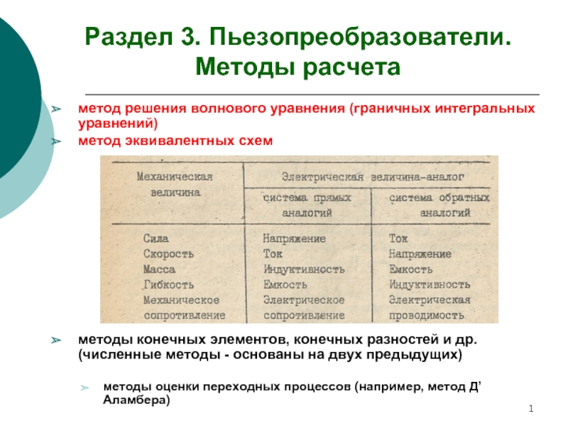
Слайд 11Напыление
Бомбардировка ионами, возможно в присутствии внешних полей: СВЧ, магнетронное, и др.
Распыляемая
мишень осаждается на подложку в вакуумной камере.
Типичная скорость напыления 0.1-0.3 мкм/мин.
Типичная температура < 150 °С.
Материалы: алюминий, титан, хром, платина, палладий, вольфрам, Al/Si и Ti/W сплавы, аморфный кремний, изоляторы, включая стекла и пьезокерамики (PZT и ZnO).
Реактивное распыление металлов с участием азота или кислорода приводит к образованию пленок таких соединений как TiN или TiO2.

Слайд 12Молекулярно-пучковая (лучевая) эпитаксия – molecular-beam epitaxy (MBE)
Схема типичной промышленной установки
 эпитаксия – molecular-beam epitaxy (MBE)Схема типичной промышленной установки")

Слайд 14Газофазная эпитаксия (Vapor Phase Epitaxy) в хлоридной системе или с использованием металло-органических
соединений
metal-organic chemical vapor deposition (MOCVD)
Схема промышленной установки MOCVD
 в хлоридной системе или с использованием металло-органических соединений metal-organic chemical")

Слайд 16Моды эпитаксиального роста
Технология молекулярно-лучевой эпитаксии (MBE) или газофазной эпитаксии с использованием
металлоорганических соединений (MOVPE, MOCVD).
Моды роста:
Франка—ван дер Мерве (Frank—van der Merve, FM)
Фолмера—Вебера (Volmer—Weber, VW)
Странского—Крастанова (Stranski—Krastanow, SK)
 или газофазной эпитаксии с использованием металлоорганических соединений (MOVPE, MOCVD).Моды")
Слайд 17Движущая сила эпитаксии – пересыщение (supersaturation) газовой фазы и адсорбционного слоя
ΔF
= kTv ln(p/pe), where k = 1.38x10⁻²³ J/K = 8.617x10⁻⁵ eV/K
 газовой фазы и адсорбционного слояΔF = kTv ln(p/pe), where")

Слайд 19Три стадии формирования наночастиц
Нуклеация (Nucleation) - Гомогенное или гетерогенное образование зародышей
новой фазы за счет флуктуаций.
Начальный рост (Initial growth) - Рост за счет обеднения прилегающих областей матрицы.
Коалесценция (Ostwald ripening) - Рост крупных частиц за счет растворения мелких частиц.
Начальный рост (Initial growth) - Рост за счет обеднения прилегающих областей матрицы.
Коалесценция (Ostwald ripening) - Рост крупных частиц за счет растворения мелких частиц.
 - Гомогенное или гетерогенное образование зародышей новой фазы за счет")
Слайд 20Поверхностная энергия
γ > 0 – коэффициент поверхностного натяжения
S – площадь поверхности
Формирование
частицы новой фазы связано с образованием поверхности раздела фаз

Слайд 21Нуклеация в объеме
Работа, необходимая для создания зародыша новой фазы
Критический зародыш
Вероятность
образования зародыша новой фазы

Слайд 22Нуклеация островка на поверхности
Young 1805
θ > 0 – распад пленки на
островки (Volmer - Weber island growth mode)
γs – γfs > γf – полное смачивание; послойный рост пленки (Frank - van der Merwe growth mode)
γs – γfs > γf – полное смачивание; послойный рост пленки (Frank - van der Merwe growth mode)


Слайд 24Давление под искривленной поверхностью
Для двух фаз, находящихся в равновесии,
γ = 1
Дж/м2
k = 1.38 10-23 Дж/К
a = ?
k = 1.38 10-23 Дж/К
a = ?
Внутри частицы новой фазы
давление повышено

Слайд 25Самоорганизация при пересыщении на поверхности
Выращивание субмонослойных островков
Распад тонких пленок на
островки
Выращивание усов (whiskers, nanowires, rods) – массивов квантовых проволок – по механизму пар-жидкость-кристалл (ПЖК)
Выращивание усов (whiskers, nanowires, rods) – массивов квантовых проволок – по механизму пар-жидкость-кристалл (ПЖК)

Слайд 26Механизм роста ПЖК
Пересыщенный пар
кристаллическая
подложка
пересыщенная жидкость
кристалл
ус
whisker
nanowire
nanorod

Слайд 27ZnO nanowires on sapphire
(a) Plan view and (b) glancing view of
ZnO nanowires grown on a-plane sapphire. The nanowires grow perpendicular to the substrate and with nearly perfect rotational alignment with respect to the substrate lattice. Scale bars are 100 nm. Baxer et. al. JCG 274, 407 (2005).
 Plan view and (b) glancing view of ZnO nanowires grown on")
Слайд 28ZnO nanostructures
Typical SEM images showing morphologies of ZnO structures:
dense filmlike
rods (a), dense filmlike nanoplatelets (c), flowerlike nanoplatelets (e), nanobelts (g), and nanowires (i).
The corresponding high magnification images are displayed in (b), (d), (f), (h), and (j), respectively. After C. Ye., X. Fang, Y. Hao, X. Teng, L. Zhang, J. Phys. Chem. B 2005;
The corresponding high magnification images are displayed in (b), (d), (f), (h), and (j), respectively. After C. Ye., X. Fang, Y. Hao, X. Teng, L. Zhang, J. Phys. Chem. B 2005;
, dense filmlike")
Слайд 29Одномерные наноструктуры
G
H
I
J
A schematic summary of the kinds of quasi-one dimensional nanostructures:
(A) Nanowires and nanorods;
(B) core–shell structures with metallic inner core, semiconductor, or metal-oxide;
(C) nanotubules/nanopipes and hollow nanorods;
(D) heterostructures;
(E) nanobelts/nanoribbons;
(F) nanotapes; (G) dendrites; (H) hierarchical nanostructures; (I) nanosphere assembly; (J) nanosprings.
(F) nanotapes; (G) dendrites; (H) hierarchical nanostructures; (I) nanosphere assembly; (J) nanosprings.
From: Kolmakov A, Moskovits M. Annu. Rev. Mater. Res. 2004;
 Nanowires and nanorods;")
Слайд 30Synthesis of core–shell nanowires
a, Gaseous reactants (red) catalytically decompose on the
surface of a gold nanocluster leading to nucleation and directed nanowire growth.
b, One-dimensional growth is maintained as reactant decomposition on the gold catalyst is strongly preferred.
c, Synthetic conditions are altered to induce homogeneous reactant decomposition on the nanowire surface, leading to a thin, uniform shell (blue). d, Multiple shells are grown by repeated modulation of reactants. (L.J. Lauhon, et al, Nature 2002.)
 catalytically decompose on the surface of a gold")
Слайд 31Si–Si homoepitaxial core–shell nanowires.
a, b, Diffraction contrast and highresolution TEM images,
respectively, of an unannealed intrinsic silicon core and p-type silicon shell nanowire grown at 450 °C. Crystal facets in the high-resolution TEM image designated by arrows indicate initially epitaxial shell growth at low temperature. Scale bars are 50 nm and 5 nm, respectively. c, d, TEM images (analogous to a and b) of an i-Si/p-Si core–shell nanowire annealed at 600 °C for 30 min after core–shell growth at 450 °C. Inset, two-dimensional Fourier transforms of the image depicting the [111] zone axis of the single crystal nanowire. The 1/3 {422} reflections, although forbidden in bulk silicon, arise as a result of the finite thickness of the nanowire. e, f, TEM images of an i-Si/SiOx/p-Si nanowire. The oxide layer is too thin (<1 nm) to discern in the high resolution image, but the sharp interface (dashed line) between the crystalline core and amorphous overcoat clearly differs from the faceting seen in b and illustrates the disruption of epitaxy. Inset, TEM image of p-Si coating the nanowire and the Au nanocluster tip. Scale bar is 50 nm. g, Three-terminal current (I ) versus voltage (V ) measurements of the nanowires described in the preceding panels. Curves b, d and f are labelled according to the representative TEM image (b, d and f) from the same sample of wires. Curve f has been multiplied by a factor of 104. Insets, current versus backgate voltage to determine field-effect mobilities.


Слайд 33Si–Ge and Si–Ge–Si core–shell nanowires.
Elemental mapping cross-section indicating a 21-nm-diameter Si
core (blue circles), 10-nm Ge shell (red circles) and <1 nm interface.
Cross-sectional elemental mapping of a double-shell structure with an intrinsic silicon core (diameter, 20 nm), intrinsic germanium inner shell (thickness, 30 nm), and p-type silicon outer shell (4 nm); silicon is blue circles and germanium is red circles.
, 10-nm")
Слайд 34Coaxially-gated nanowire transistors
a, Device schematic showing transistor structure. The inset shows
the cross-section of the as-grown nanowire, starting with a p-doped Si core (blue, 10 nm) with subsequent layers of i-Ge (red, 10 nm), SiOx (green, 4 nm), and p-Ge (5 nm). The source (S) and drain (D) electrodes are contacted to the inner i-Ge core, while the gate electrode (G) is in contact with the outer p-Ge shell and electrically isolated from the core by the SiOx layer.
b, Scanning electron micrograph (SEM) of a coaxial transistor. Source and drain electrodes were deposited after etching the Ge (30% H2O2, 20 s) and SiOx layers (buffered HF, 10 s) to expose the core layers. The etching of these outer layers is shown clearly in the inset and is indicated by the arrow. The gate electrodes were defined in a second step without any etching before contact deposition. Scale bar is 500 nm.
c, Gate response of the coaxial transistor at VSD = 1 V, showing a maximum transconductance of 1500 nA/ V. Charge transfer from the p-Si core to the i-Ge shell produces a highly conductive and gateable channel.

Слайд 35Домашнее задание
Ландау, Лифшиц. Статистическая физика. Часть 1. Параграфы 160 - 162.
Теория нуклеации.
Определить размеры критических зародышей и давление в них: 1) в газовой фазе
2) в конденсированной среде
3) для критического островка, имеющего форму сферического сегмента, на плоской поверхности этой среды.
Коэффициенты поверхностного натяжения материала новой фазы γf = 1 Дж/м2 ; исходной среды γs = 0.5 Дж/м2; границы раздела γfs = 0.2 Дж/м2
Пересыщение с/сeq = 1.1.
Температура = 727оС
Радиус молекулы = 1 Å