- Главная
- Разное
- Дизайн
- Бизнес и предпринимательство
- Аналитика
- Образование
- Развлечения
- Красота и здоровье
- Финансы
- Государство
- Путешествия
- Спорт
- Недвижимость
- Армия
- Графика
- Культурология
- Еда и кулинария
- Лингвистика
- Английский язык
- Астрономия
- Алгебра
- Биология
- География
- Детские презентации
- Информатика
- История
- Литература
- Маркетинг
- Математика
- Медицина
- Менеджмент
- Музыка
- МХК
- Немецкий язык
- ОБЖ
- Обществознание
- Окружающий мир
- Педагогика
- Русский язык
- Технология
- Физика
- Философия
- Химия
- Шаблоны, картинки для презентаций
- Экология
- Экономика
- Юриспруденция
Changes to LPDIMM Rev 02 презентация
Содержание
- 1. Changes to LPDIMM Rev 02
- 2. 1. general A. Please fix all dangling
- 3. 2. Component: nets in all design Please
- 4. 2. Component: nets in all design(cont.)
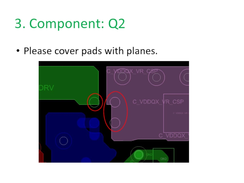
- 5. 3. Component: Q2 Please cover pads with planes.
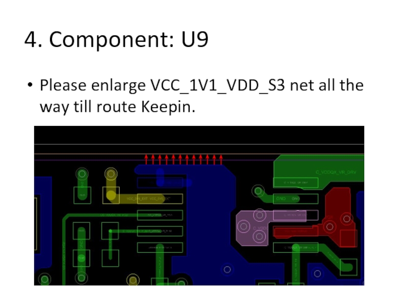
- 6. 4. Component: U9 Please enlarge VCC_1V1_VDD_S3 net all the way till route Keepin.
- 7. 5. New MASK for VIA_FILL Please prepare
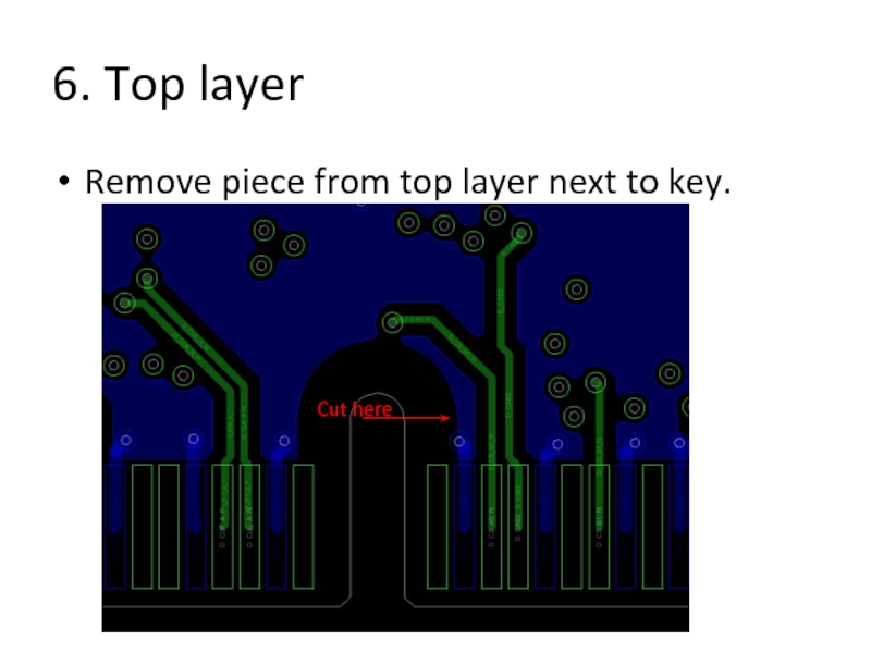
- 8. 6. Top layer Remove piece from top layer next to key. Cut here
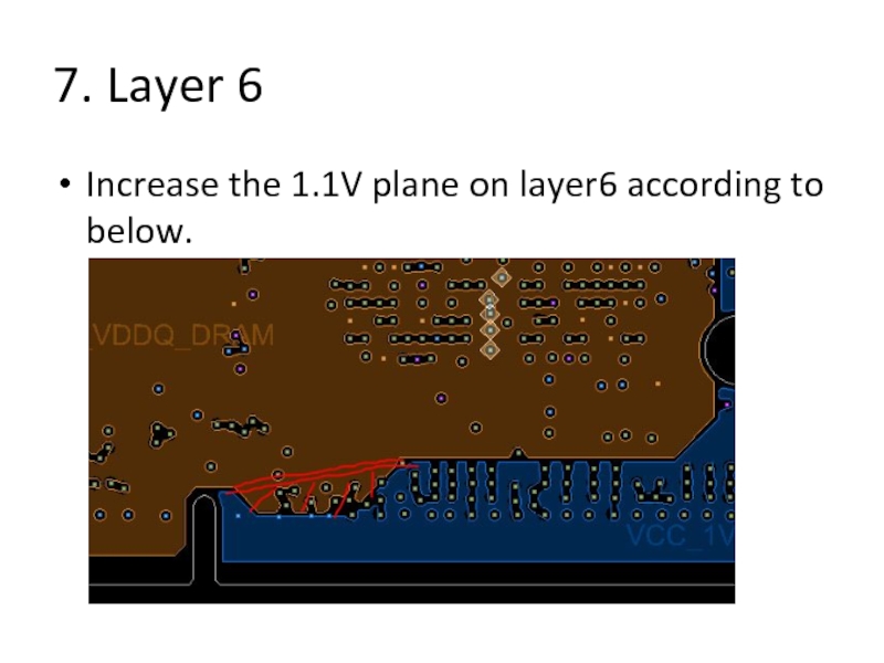
- 9. 7. Layer 6 Increase the 1.1V plane on layer6 according to below.
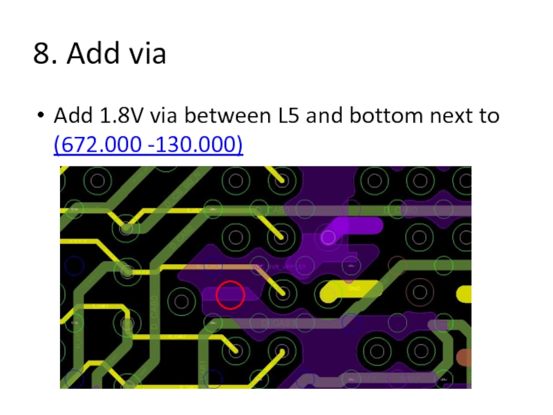
- 10. 8. Add via Add 1.8V via
- 11. 9. Component Q2, R36 Define R36 pad
- 12. 10. Turn CSP and CSN pins in
- 13. 11. Enlarge VDDQ_DRAM rail. Rotate C102 90
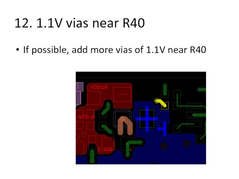
- 14. 12. 1.1V vias near R40 If possible, add more vias of 1.1V near R40
- 15. 13. 1.1V/VPP TP Route a trace from
- 16. 14. Silk - TOP Fix REFDES for
- 17. 15. Silk - BOTTOM Change PCB PN
- 18. 16. New placement The next slide shows
- 19. 16. New placements (cont.)
Слайд 21. general
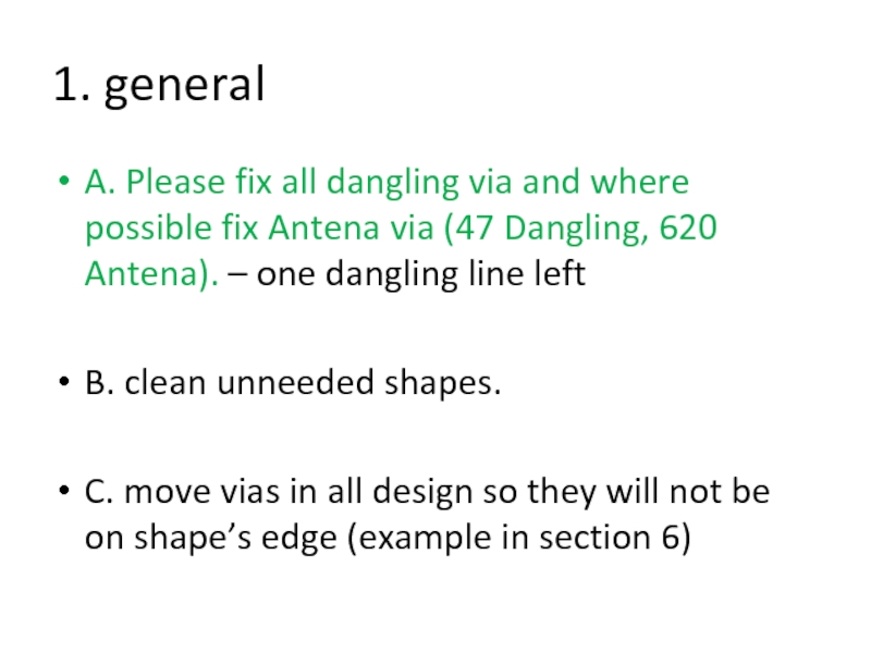
A. Please fix all dangling via and where possible fix
Antena via (47 Dangling, 620 Antena). – one dangling line left
B. clean unneeded shapes.
C. move vias in all design so they will not be on shape’s edge (example in section 6)
B. clean unneeded shapes.
C. move vias in all design so they will not be on shape’s edge (example in section 6)
Слайд 32. Component: nets in all design
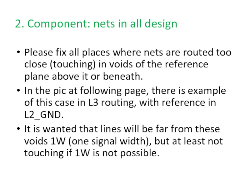
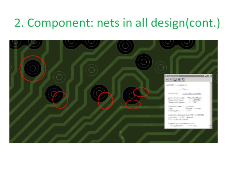
Please fix all places where nets
are routed too close (touching) in voids of the reference plane above it or beneath.
In the pic at following page, there is example of this case in L3 routing, with reference in L2_GND.
It is wanted that lines will be far from these voids 1W (one signal width), but at least not touching if 1W is not possible.
In the pic at following page, there is example of this case in L3 routing, with reference in L2_GND.
It is wanted that lines will be far from these voids 1W (one signal width), but at least not touching if 1W is not possible.
Слайд 75. New MASK for VIA_FILL
Please prepare new mask called VIA_FILL.
This mask
will contain all vias only in the DRAM BGA TOP layer.
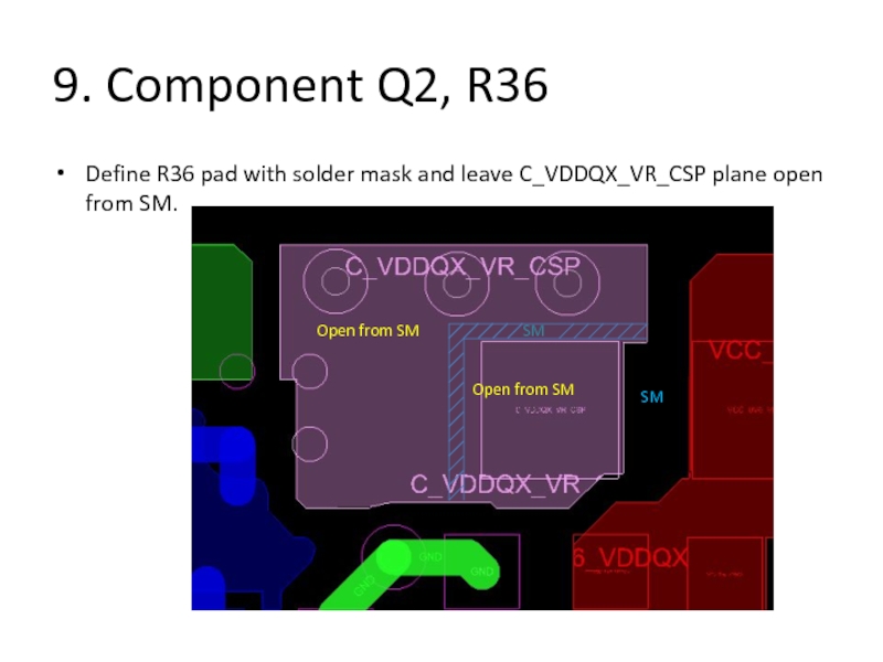
Слайд 119. Component Q2, R36
Define R36 pad with solder mask and leave
C_VDDQX_VR_CSP plane open from SM.
SM
Open from SM
Open from SM
SM
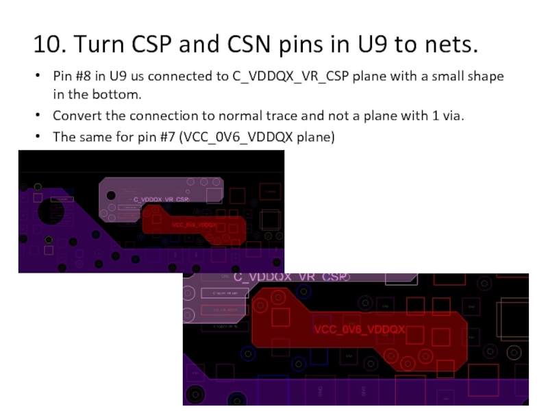
Слайд 1210. Turn CSP and CSN pins in U9 to nets.
Pin #8
in U9 us connected to C_VDDQX_VR_CSP plane with a small shape in the bottom.
Convert the connection to normal trace and not a plane with 1 via.
The same for pin #7 (VCC_0V6_VDDQX plane)
Convert the connection to normal trace and not a plane with 1 via.
The same for pin #7 (VCC_0V6_VDDQX plane)
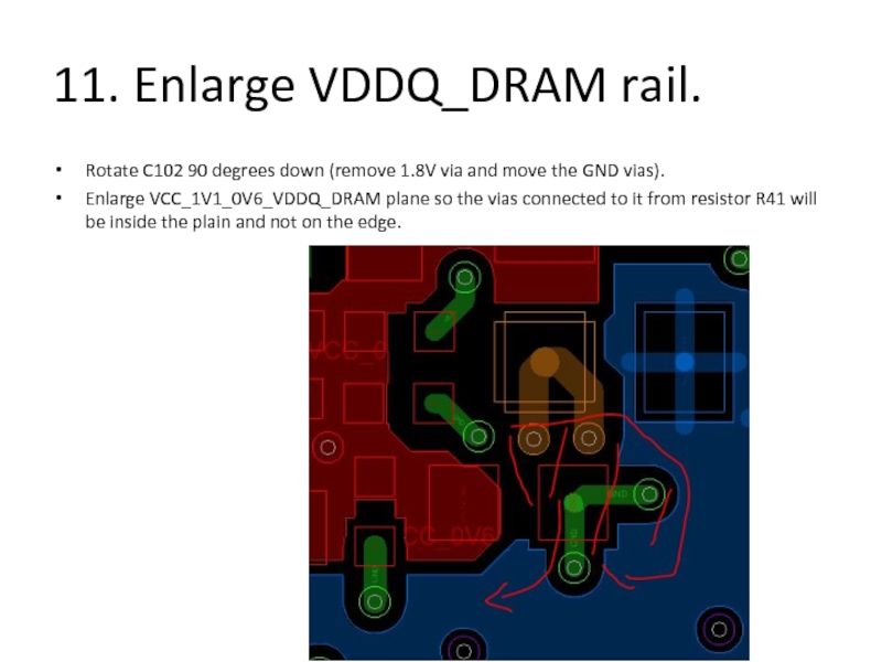
Слайд 1311. Enlarge VDDQ_DRAM rail.
Rotate C102 90 degrees down (remove 1.8V via
and move the GND vias).
Enlarge VCC_1V1_0V6_VDDQ_DRAM plane so the vias connected to it from resistor R41 will be inside the plain and not on the edge.
Enlarge VCC_1V1_0V6_VDDQ_DRAM plane so the vias connected to it from resistor R41 will be inside the plain and not on the edge.
Слайд 1513. 1.1V/VPP TP
Route a trace from DRAM to 1.1V and VPP
TP instead of direct connection to the plane.
If impossible, try at least to do that for 1.1V (TP11 and TP15)
If impossible, try at least to do that for 1.1V (TP11 and TP15)
Слайд 1614. Silk - TOP
Fix REFDES for new components. And old components
that moved.
Fix silk of TP that moved.
Change card name (LPDIMM_LP4_200B) to: LP4/x_200B (CNL U)
Fix silk of TP that moved.
Change card name (LPDIMM_LP4_200B) to: LP4/x_200B (CNL U)
Слайд 1816. New placement
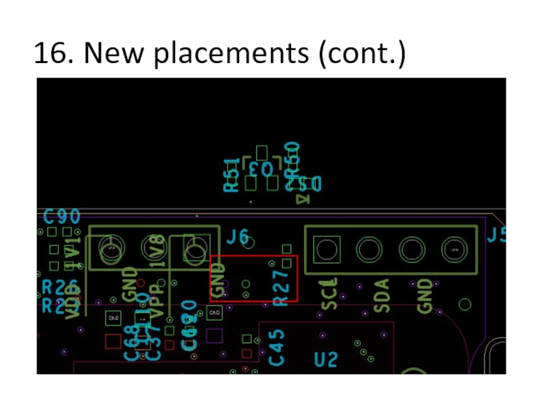
The next slide shows basic placement.
Please move: TP17, TP18,
J6, R27.
Please move J5 (4 pin header) a little to the right.
Place new components in the red square area.
It doesn’t have to be exactly like I requested. It can be changed a little bit as long as everything fit.
Please move J5 (4 pin header) a little to the right.
Place new components in the red square area.
It doesn’t have to be exactly like I requested. It can be changed a little bit as long as everything fit.

